GaN-base LED epitaxial structure and growing method thereof

An epitaxial structure and growth method technology, applied in electrical components, circuits, semiconductor devices, etc., can solve the problems of large quantum barrier thickness, long barrier time, and increase material production costs, and achieve high luminous efficiency and low growth costs. Effect

Inactive Publication Date: 2013-09-25
AQUALITE CO LTD
View PDF5 Cites 7 Cited by
  • Summary
  • Abstract
  • Description
  • Claims
  • Application Information

AI Technical Summary

Problems solved by technology

This growth method takes a long time to raise and lower the temperature between the well and the barrier and grow the barrier, and the cost is high. The contradiction between the temperature difference between the well and the barrier and the crystal quality of the active region is prominent.
[0004] Usually in the MQW of GaN-based LEDs, the thickness of QW (Quantum Wells, quantum well) is about 3nm (nano), the thickness of the quantum barrier is 10nm to 15nm, and the quantum barrier is usually a mixed atmosphere of H2 (hydrogen gas) and N2 (nitrogen gas), The growth temperature is 80 degrees Celsius (°C) to 150°C higher than that of the quantum well, and the heating and cooling time is too long and the thickness of the quantum barrier is too large, which will inevitably increase the production cost of the material

Method used


Image

  • GaN-base LED epitaxial structure and growing method thereof

Examples


Embodiment Construction

[0021] The principles and features of the present invention are described below in conjunction with the accompanying drawings, and the examples given are only used to explain the present invention, and are not intended to limit the scope of the present invention.

[0022] In the embodiment of the present invention, the method for growing the epitaxial structure of GaN-based LED may include the following steps:

[0023] Step 1, sequentially growing a GaN nucleation layer, an unintentionally doped u-GaN layer, and an N-type doped GaN layer on a sapphire substrate;

[0024] Wherein, the growth temperature of the GaN nucleation layer is 550° C. to 680° C., and the thickness is 20 nm to 70 nm.

[0025] Wherein, the growth temperature of the unintentionally doped u-GaN layer is above 1100° C., and the thickness is 1 μm (micrometer) to 5 μm.

[0026] Herein, the range of A to B means within the range of A and B, and this range may include the two end values ​​of A and B, or may not ...


PUM


Abstract

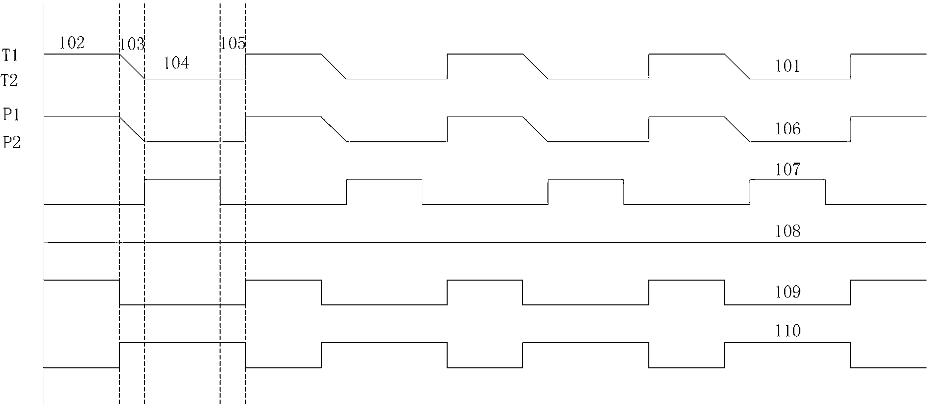
The invention relates to a GaN-base LED epitaxial structure and a growing method of the GaN-base LED epitaxial structure. The growing method of the GaN-base LED epitaxial structure includes the following steps: (1) sequentially growing a GaN nucleating layer, an involuntary doping u-GaN layer and an N-type doping GaN layer on a sapphire substrate, (2) growing an active area MQW layer on the N-type doping GaN layer, when the active area MQW layer grows, enabling the pressure of a reaction chamber during quantum well growth to be smaller than the pressure of the reaction chamber during quantum base growth, keeping a pure N2 atmosphere for set time respectively before the quantum well growth and after the quantum well growth, controlling the growth thickness of a quantum base in the active area MQW layer to be smaller than 6nm, and (3) further growing an electronic barrier layer, a P-type doping GaN layer and a contact layer on the active area MQW layer sequentially. The GaN-base LED epitaxial structure is low in production cost, and a GaN-base LED manufactured by the GaN-base LED epitaxial structure is high in luminous efficiency.

Description

technical field [0001] The invention relates to the field of optoelectronics, in particular to an epitaxial structure of a GaN-based LED and a growth method thereof. Background technique [0002] LED (Light Emitting Diode, Light Emitting Diode) has the advantages of small size, sturdy and durable, strong controllability of luminous band, high luminous efficiency, low heat loss, low light decay, energy saving, environmental protection, etc., and has been widely used. In recent years, LEDs have been widely used in display screens, instrument backlights, traffic signal displays, automobile taillights, interior instrument display and decoration, and lighting. However, the popularization of LED lighting needs further improvement of its brightness and further reduction of production cost. [0003] At present, traditional GaN-based LEDs are made of sapphire (chemical formula Al 2 o 3 , aluminum oxide) substrate using MOCVD (Metal-Organic Chemical Vapor Deposition, metal organic ...

Claims


Application Information

Patent Timeline
Patent Type & Authority Applications(China)
IPC IPC(8): H01L33/06H01L33/00
Inventor 罗绍军艾常涛靳彩霞董志江
Owner AQUALITE CO LTD
Why Eureka
Try Eureka