Method for preparing mesoporous silicon nanowire by metal nanoparticle auxiliary etching method

A metal nanoparticle and assisted etching technology, which is applied in the coating process of metal materials, the manufacturing of microstructure devices, and the process for producing decorative surface effects, etc., can solve the problems of large-scale integration difficulties, high equipment requirements, and high costs. , to achieve the effect of low cost, huge specific surface area and simple process

Active Publication Date: 2013-10-09
KUNMING UNIV OF SCI & TECH
View PDF5 Cites 17 Cited by
  • Summary
  • Abstract
  • Description
  • Claims
  • Application Information

AI Technical Summary

Problems solved by technology

Silicon nanowires obtained by this method are usually randomly distributed, which makes large-scale integration difficult
"Top-down" refers to starting from bulk materials and using thin film growth or nano-lithography technology to prepare nanowire materials. The silicon nanowires obtained by this method have high precision, but they also have high requirements for equipment, high cost, and Low efficiency and other disadvantages

Method used


Image

  • Method for preparing mesoporous silicon nanowire by metal nanoparticle auxiliary etching method
  • Method for preparing mesoporous silicon nanowire by metal nanoparticle auxiliary etching method
  • Method for preparing mesoporous silicon nanowire by metal nanoparticle auxiliary etching method

Examples


Embodiment 1

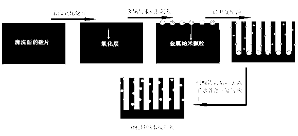
[0024] (1) Silicon wafer pretreatment: ultrasonically clean the monocrystalline silicon wafer (100) with a resistivity of 0.01-0.09Ω·cmp with commercially available analytically pure acetone, toluene, ethanol, and deionized water for 10 minutes in sequence;

[0025] (2) Oxidation treatment of the surface of the silicon wafer: the silicon wafer pretreated in step (1) is oxidized on the surface by conventional thermal oxidation to form an oxide layer, and the existence of the oxide layer is formed by utilizing the mesoporous structure;

[0026] (3) Preparation of corrosion solution: AgNO with a concentration of 1mol / L 3 Solution, hydrofluoric acid with a mass concentration of 10%, H with a concentration of 3mol / L 2 o 2 The corrosion solution is obtained by mixing at a volume ratio of 1:8:1;

[0027] (4) Preparation of mesoporous silicon nanometers: place the silicon wafer treated with surface oxidation in step (2) in the corrosion solution obtained in step (3) in a dark room t...

Embodiment 2

[0029] (1) Silicon wafer pretreatment: the p-type monocrystalline silicon wafer (111) with a resistivity of 10-100 Ω·cm was ultrasonically cleaned for 10 minutes with commercially available analytically pure acetone, toluene, ethanol, and deionized water in sequence;

[0030] (2) Oxidation treatment on the surface of the silicon wafer: the silicon wafer pretreated in step (1) is subjected to surface oxidation treatment by conventional chemical oxidation to form an oxide layer, and the existence of the oxide layer can utilize the formation of a mesoporous structure;

[0031] (3) Preparation of corrosion solution: KAuCl with a concentration of 1mol / L 4 solution), hydrofluoric acid with a mass concentration of 10%, and HNO with a concentration of 5mol / L 3 5:10:10 is mixed by volume to obtain corrosion solution;

[0032] (4) Preparation of mesoporous silicon nanometers: place the silicon wafer treated with surface oxidation in step (2) in the corrosion solution obtained in step (...

Embodiment 3

[0034] (1) Silicon wafer pretreatment: the n-type single crystal silicon wafer (111) with a resistivity of 0.01Ω·cm was ultrasonically cleaned with commercially available analytically pure acetone, toluene, ethanol, and deionized water for 30 minutes in sequence;

[0035] (2) Oxidation treatment on the surface of the silicon wafer: the silicon wafer pretreated in step (1) is subjected to surface oxidation treatment by conventional electrochemical oxidation to form an oxide layer, and the existence of the oxide layer can utilize the formation of a mesoporous structure;

[0036] (3) Preparation of corrosion solution: HAuCl with a concentration of 1mol / L 4 Solution, hydrofluoric acid with a mass concentration of 30%, Fe(NO with a concentration of 10mol / L 3 ) 3 The corrosion solution is obtained by mixing in a volume ratio of 0.01:0.01:0.2;

[0037] (4) Preparation of mesoporous silicon nanometers: place the silicon wafer treated with surface oxidation in step (2) in the corrosi...


PUM

PropertyMeasurementUnit
electrical resistivityaaaaaaaaaa

Abstract

The invention provides a method for preparing mesoporous silicon nanowire by metal nanoparticle auxiliary etching method, and belongs to the technical field of semiconductor materials. The method comprises the following steps: pretreating a silicon wafer; performing surface oxidation treatment; placing the treated silicon wafer in corrosive liquid; then soaking in nitrate solution; washing by using a large number of deionized water; and carrying out blow-drying by nitrogen to obtain the mesoporous silicon nanowire. Compared with the general compact silicon nanowire, the mesoporous silicon nanowire prepared by the method contains a large amount of holes with diameters of 2 to 50 nm, and the mesoporous silicon nanowire maintains a certain single crystal characteristic, so that the mesoporous silicon nanowirehas huger specific surface area and embodies unique optical and electrical properties, and the mesoporous silicon nanowire has great application prospect in the fields of nano sensors, optical devices, nano catalysis and the like.

Description

technical field [0001] The invention belongs to the technical field of semiconductor materials, and in particular relates to a preparation method of mesoporous silicon nanowires. Background technique [0002] In recent years, nanomaterials have aroused widespread research interest due to their unique physical and chemical properties and potential application prospects in many fields. Among them, silicon nanowires, as a new type of semiconductor material, exhibit novel physical properties such as quantum confinement effect, surface effect, and quantum confinement effect with the continuous reduction of diameter, which makes them used in light, electricity, heat, etc. , magnetism, and catalytic reactions show significantly different physical properties from other materials, so they show very important application potential in the fields of photoluminescence, large-scale integrated circuits, single electronic devices, and nanosensors. [0003] The preparation of silicon nanowi...

Claims


Application Information

Patent Timeline
Patent Type & Authority Applications(China)
IPC IPC(8): B81C1/00
Inventor 马文会李绍元周阳魏奎先谢克强伍继君秦博刘大春杨斌戴永年
Owner KUNMING UNIV OF SCI & TECH
Why Eureka
Try Eureka