
Method for detecting under-etching and deficiency defect of through hole

A technology for insufficient etching and detection of through holes, which is used in semiconductor/solid-state device testing/measurement, electrical components, semiconductor/solid-state device manufacturing, etc. question

Active Publication Date: 2013-10-23
SHANGHAI HUALI MICROELECTRONICS CORP
View PDF5 Cites 9 Cited by
  • Summary
  • Abstract
  • Description
  • Claims
  • Application Information

AI Technical Summary

Problems solved by technology

For example, in the etching process of etching the hard mask (Hard Mask Etch) first and then etching the through hole (All in One Etch), the under-etching defects are often affected by the cleaning process after the hard mask etching, the through hole etching itself and the photolithography of the through hole etching. The common influence of the process, when some of the process windows are not optimized enough, defects will appear and become a major killer that restricts the improvement of yield rate
[0003] The detection of under-etching defects in the back-stage through holes is one of the recognized problems in the industry. There are usually two detection methods used in the industry: one is to use an electron beam defect scanner to inspect after the cleaning process after etching, but due to the existence of Due to the influence of the Faraday cup, the detection capture rate is usually very low and the accuracy is not high; the second is to do the detection after the copper filling is flattened, but because most of the through holes are connected by copper wires, the through holes that can be detected Insufficient defects are only 3 / 7, and affected by the front layer PMOS / NMOS, the signal of insufficient via defects on NMOS will be weaker
These two methods have great deficiencies, and it is difficult to provide effective reference for online process window optimization

Method used


Image

  • Method for detecting under-etching and deficiency defect of through hole
  • Method for detecting under-etching and deficiency defect of through hole
  • Method for detecting under-etching and deficiency defect of through hole

Examples


Embodiment Construction

[0027] In order to make the content of the present invention clearer and easier to understand, the content of the present invention will be described in detail below in conjunction with specific embodiments and accompanying drawings.

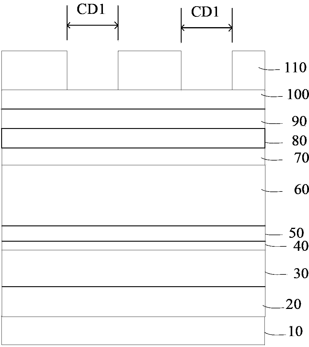
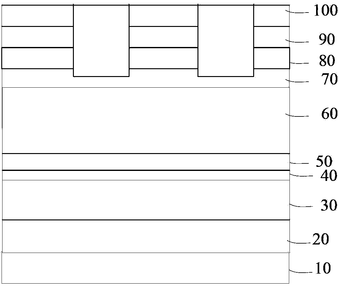
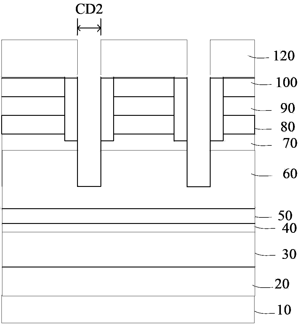
[0028] The present invention aims at etching the hard mask (Hard Mask Etch) first and then etching the through hole (All in One Etch). The following technical principle is applied to grow metal silicide on the wafer with PMOS structure as the substrate, and The thickness of the dielectric layer that needs to be consumed when etching the through hole in the growth etching process, the same mask is used for the hard mask etching and the through hole etching, and the electron beam defect scanner is used for inspection after the copper filling is planarized. The specific implementation steps are as follows:

[0029] Firstly, the surface of the wafer is implanted with N-type well region ions and P-type source-drain ions by non-photoresist ion implant...


PUM


Abstract

The invention discloses a method for detecting the under-etching and the deficiency defect of a through hole. The method comprises the following steps of implementing a structure that a PMOS (P-channel metal oxide semiconductor) device is arranged in an N well; growing metal silicide on a wafer according to a normal process manufacturing procedure, forming a barrier layer, and depositing a first dielectric layer and a second dielectric layer between metals; sequentially forming a hard mask, a silicon oxide and an antireflection layer on the second dielectric layer, and a hard mask etching photomask on the antireflection layer, wherein a through hole etching photomask is used as the hard mask etching photomask; completely etching the antireflection layer, the silicon oxide and the hard mask by utilizing the hard mask etching photomask, and partially etching the second dielectric layer; removing the hard mask etching photomask, and filling the antireflection layer, the silicon oxide, the hard mask and the second dielectric layer; performing etching by utilizing the through hole etching photomask until the first dielectric layer is partially etched, and removing the through hole etching photomask; removing the antireflection layer and a material, wherein the material is filled in the antireflection layer, and is the same as that of the antireflection layer; and performing etching until the barrier layer is etched through.

Description

technical field [0001] The present invention relates to the field of semiconductor manufacturing, and more particularly, the present invention relates to a method for detecting under-etched vias and missing vias. Background technique [0002] With the development of integrated circuit technology and the scaling down of critical dimensions, the etching of copper connection vias in the back-end process of semiconductor devices is insufficient (such as figure 1 shown) and missing via defects (such as figure 2 Shown) has increasingly become one of the bottlenecks in the development of integrated circuits. For example, in the etching process of etching the hard mask (Hard Mask Etch) first and then etching the through hole (All in One Etch), the under-etching defects are often affected by the cleaning process after the hard mask etching, the through hole etching itself and the photolithography of the through hole etching. The common influence of the process, when some of the pr...

Claims


Application Information

Patent Timeline
Patent Type & Authority Applications(China)
IPC IPC(8): H01L21/66H01L21/768
Inventor 范荣伟龙吟倪棋梁陈宏璘
Owner SHANGHAI HUALI MICROELECTRONICS CORP
Learn More