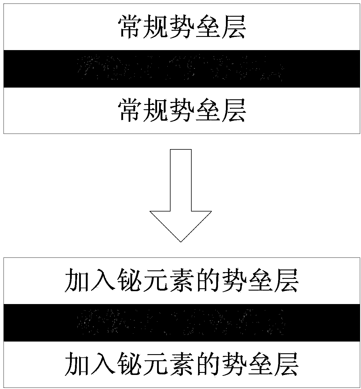
Rare bismuth semiconductor quantum well structure improved in heat stability and preparation method for rare bismuth semiconductor quantum well structure
A technology of thermal stability and quantum well, which is applied in semiconductor devices, electrical components, circuits, etc., can solve the problems of no improvement in the structure and method of the thermal stability of dilute bismuth semiconductor quantum wells, and the reduction of bismuth element content, so as to achieve easy control , Improve thermal stability, simple operation process
- Summary
- Abstract
- Description
- Claims
- Application Information
AI Technical Summary
Problems solved by technology
Method used
Image

Examples
Embodiment 1
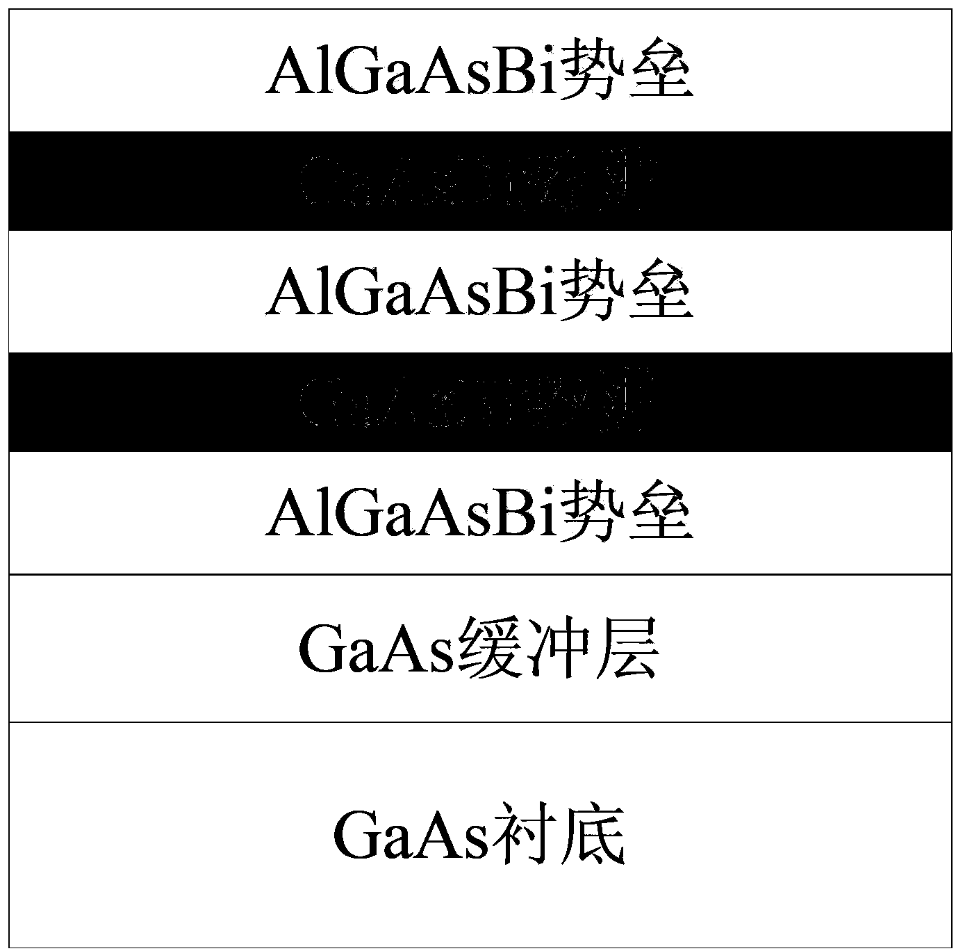
[0024] The following takes the preparation process of GaAsBi / AlGaAs double quantum well on GaAs substrate as an example to illustrate the structure and preparation steps of improving the thermal stability of the quantum well by adding bismuth element in the potential barrier. These structures and preparation steps can be directly extended to other types Dilute bismuth semiconductor quantum wells. Concrete structure and preparation steps are as follows:
[0025] (1) First grow a 100nm GaAs buffer layer on the GaAs substrate;
[0026] (2) Growth of 15nm AlGaAsBi barrier layer;
[0027] (3) Keep the shutters of the Ga, As and Bi beam source furnaces open, close the shutter of the Al beam source furnace, and grow a 10nm GaAsBi potential well layer;
[0028] (4) Continue to grow a 15nm AlGaAsBi barrier layer and a 10nm GaAsBi potential well layer;
[0029] (5) Finally, a 15nm AlGaAsBi barrier layer is grown to complete the growth of the dilute bismuth double quantum well structu...
PUM
| Property | Measurement | Unit |
|---|---|---|
| band gap temperature coefficient | aaaaa | aaaaa |
Abstract
Description
Claims
Application Information