Manufacturing method of semiconductor element
A manufacturing method and semiconductor technology, applied in semiconductor/solid-state device manufacturing, electrical components, circuits, etc., can solve the problems of difficult integration of manufacturing processes and complex manufacturing process steps.
- Summary
- Abstract
- Description
- Claims
- Application Information
AI Technical Summary
Problems solved by technology
Method used
Image
Examples
no. 1 example
[0063] The temporary material layer can be a sacrificial spacer in the selective epitaxial growth process. The selective epitaxial growth process can introduce stress into the gate channel, which is a technical means to improve carrier mobility. For example, after the sacrificial spacer is formed, a silicon germanium (SiGe) layer is selectively epitaxially grown in the cavity in the semiconductor substrate adjacent to the sacrificial spacer to form a compressive strained channel to increase hole migration. rate, or to form a silicon carbide layer to form a tensile strain channel (tensile strained channel) to increase electron mobility.
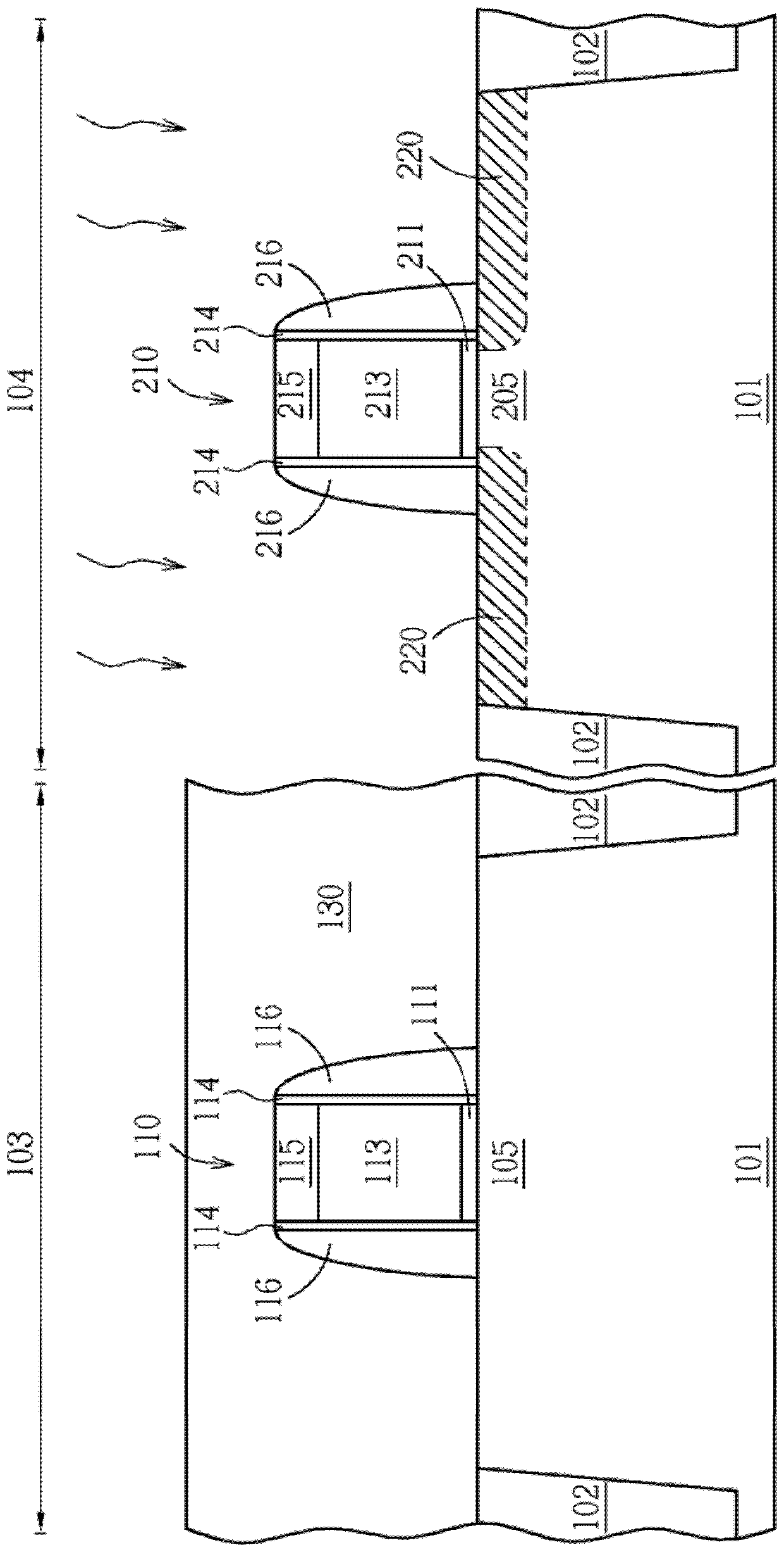
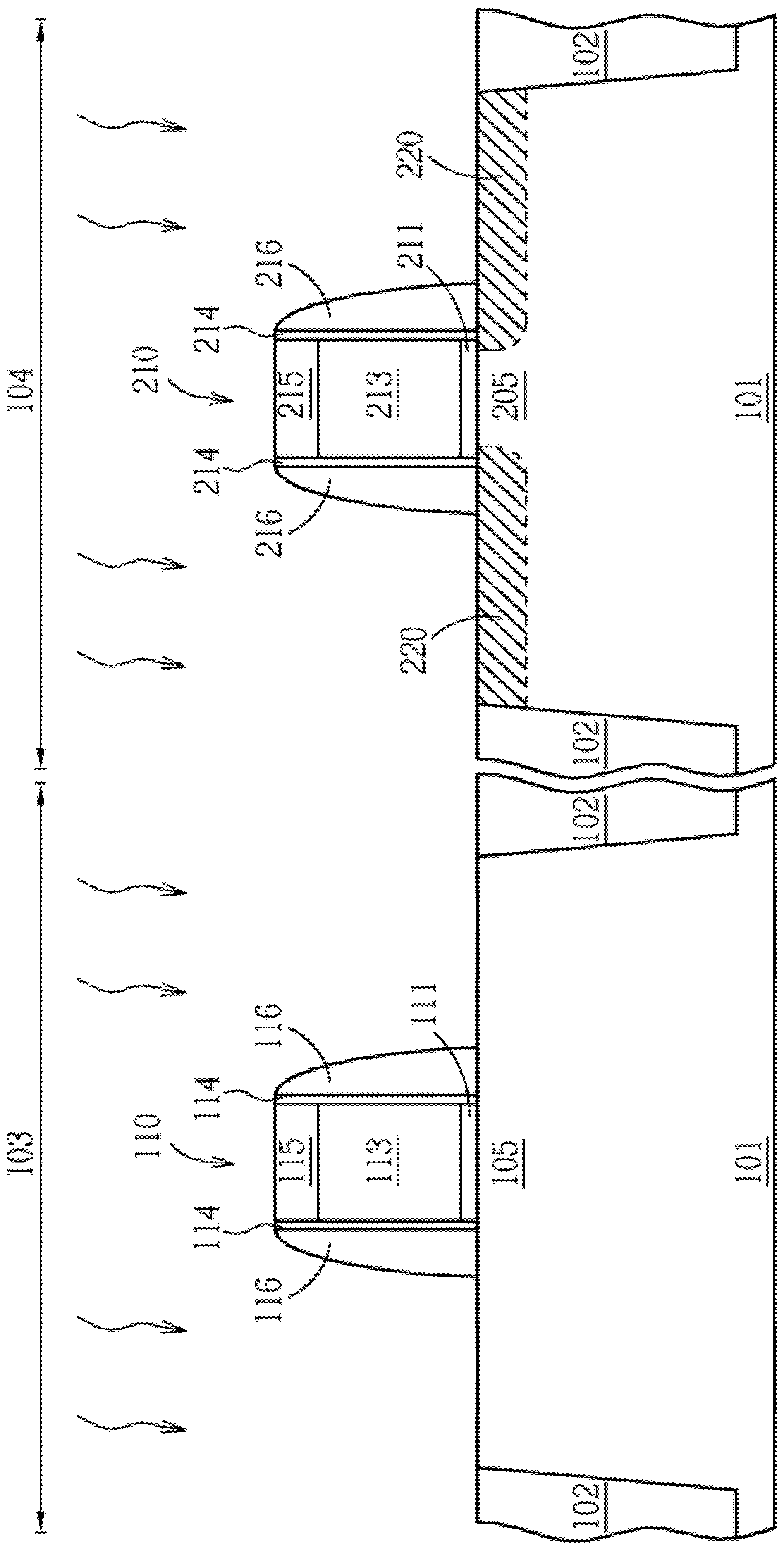
[0064] Figure 6 to Figure 8 It is shown that the temporary material layer of the present invention is used as a sacrificial spacer in the selective epitaxial growth process. First, if Figure 6 As shown, a material layer 140 is uniformly and blanketly covering the substrate 101 , the STI 102 , the gate structure 110 / 210 and the spacers 1...
no. 2 example
[0071] The temporary material layer may also be a stress providing layer in stress memorization technique (SMT). Generally speaking, this method of introducing stress into MOS transistors is the so-called stress memory technology, which usually includes the following steps: (1) performing a pre-amorphization (pre-amorphization implant, PAI) manufacturing process on the surface of the silicon substrate Forming an amorphous silicon layer; (2) then depositing a stress layer on the silicon substrate; (3) then performing a heat treatment process so that the silicon substrate can remember the stress imposed on it by the stress layer; and (4) removing stress layer.
[0072] Figure 9 to Figure 11 It shows that the temporary material layer of the present invention is used as a stress providing layer in the stress memory technology. First, if Figure 9 As shown, a pre-amorphization doping step is performed to form an amorphization region 153 . If the epitaxial material 152 is not d...
no. 3 example
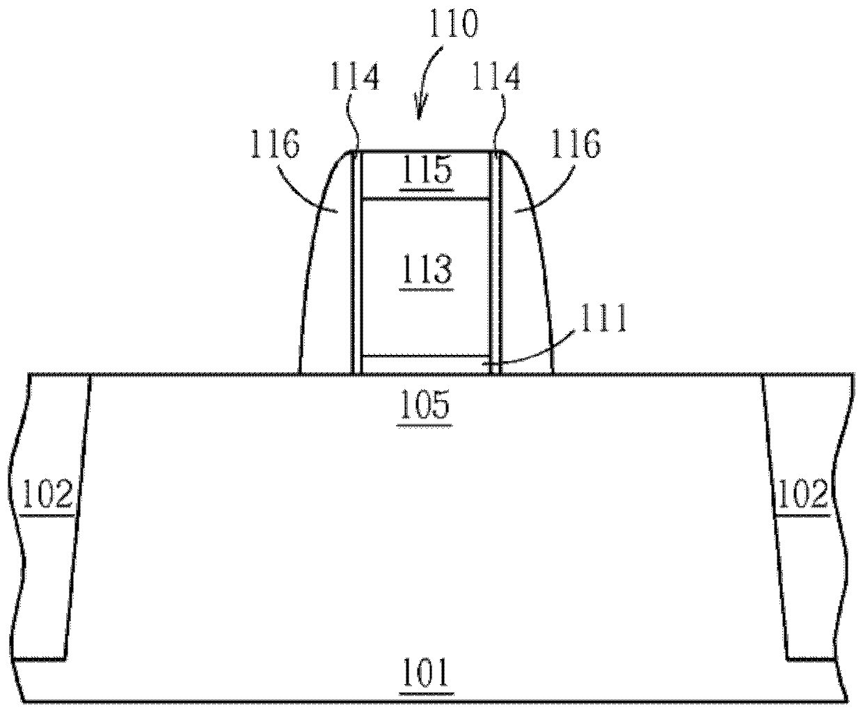
[0078] figure 1 , Figure 12 to Figure 17 Another embodiment of the semiconductor device manufacturing method of the present invention is shown. In this example, there is no photoresist on the semiconductor substrate. First, if figure 1 As shown, a substrate 101 without photoresist is provided. There may be shallow trench isolation 102 in the substrate 101, there may be a gate structure 110 on the substrate 101, a first material layer 116 on the gate structure 110, and other optional components, but there is no light on the substrate 101. cause resist. The region 109 can be one of a PMOS region or an NMOS region.
[0079] The details of the gate structure 110 can refer to the previous description, which generally includes a gate dielectric layer 111, a high dielectric constant layer (not shown), a barrier layer (not shown), and a gate material layer 113 , a hard mask 115 and a first material layer 116 . For example, the layer of temporary material may be a hard mask 11...
PUM
 Abstract
Description
Claims
Application Information


