A method for preparing a patterned sapphire substrate for gan growth

A patterned sapphire and sapphire substrate technology, applied in the direction of electrical components, circuits, semiconductor devices, etc., can solve problems such as uneven corrosion, silicon dioxide shedding, pinholes and imprints, so as to avoid local shedding and reduce dislocations Density, the effect of avoiding uneven corrosion

Active Publication Date: 2016-06-29
广东中图半导体科技股份有限公司
View PDF5 Cites 0 Cited by
  • Summary
  • Abstract
  • Description
  • Claims
  • Application Information

AI Technical Summary

Problems solved by technology

However, when the above-mentioned silicon dioxide mask is etched with BOE solution, defects such as uneven etching, partial peeling of silicon dioxide, pinholes and imprints are prone to occur.

Method used


Image

  • A method for preparing a patterned sapphire substrate for gan growth
  • A method for preparing a patterned sapphire substrate for gan growth
  • A method for preparing a patterned sapphire substrate for gan growth

Examples


Embodiment

[0038] Embodiment, preparation patterned sapphire substrate II (through pretreatment)

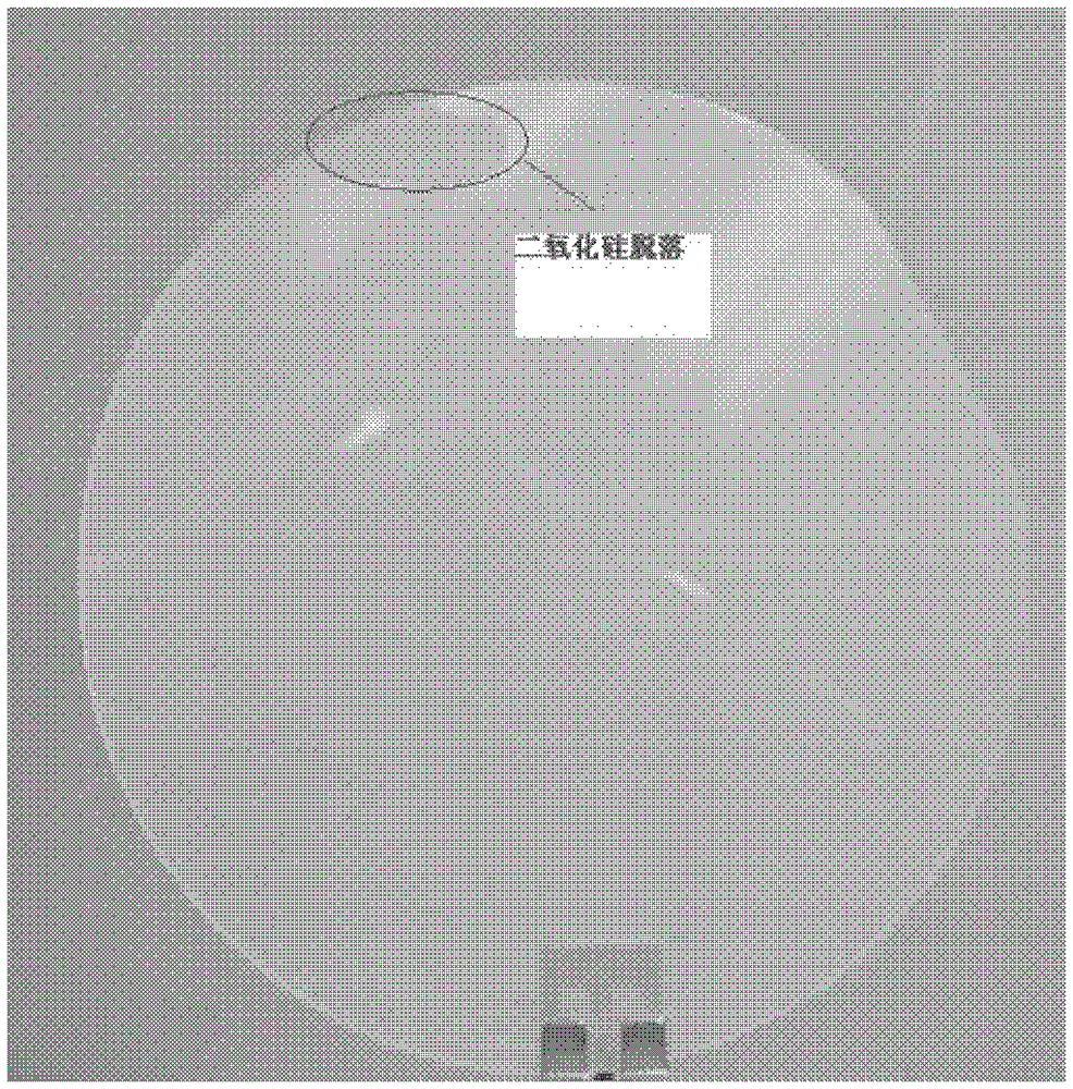
[0039] A silicon dioxide mask layer with a thickness of 0.1-1.0 μm is prepared on the C-plane sapphire by using plasma enhanced chemical vapor deposition (PECVD).

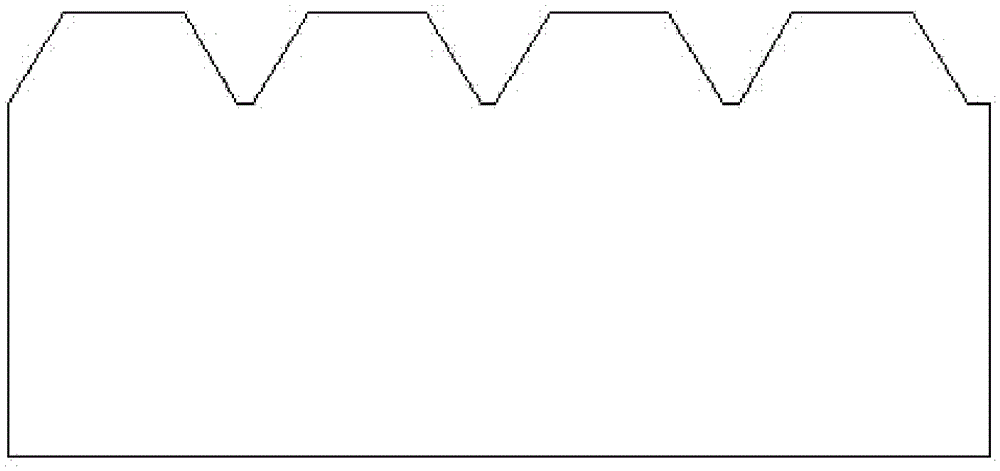
[0040] Using photolithography technology, on the silicon dioxide mask layer, periodically arranged cylindrical photoresist mask patterns with a thickness of 1.0-3.0 μm and a bottom diameter of 2.0-4.0 μm are carved. The pitch is 0.5-1.0 μm.

[0041] Put the substrate into a special buffer solution, soak it at 23-50°C for 30s, let the buffer fully wet the substrate, then take out the substrate (do not need to dry it), the concentration of the special buffer solution is: It is obtained by mixing 40% hydrofluoric acid solution and water at a volume ratio of 10:1 to 20:1.

[0042] Then put the pretreated substrate into a mixture of hydrofluoric acid solution and water with a volume ratio of 1:6 and a concentration of 40%, etch at ...


PUM

PropertyMeasurementUnit
thicknessaaaaaaaaaa
thicknessaaaaaaaaaa
heightaaaaaaaaaa

Abstract

The invention discloses a method for preparing a graphic sapphire substrate for GaN growth. Firstly, a SiO2 thin film is prepared on a sapphire substrate, graphic optical resist serves as a mask, the SiO2 is etched through a BOE solution, and a SiO2 mask graph is formed; then wet etching is conducted on the sapphire substrate, and the graphic sapphire substrate is obtained. The method is characterized in that before the SiO2 is etched through the BOE solution, the substrate is placed into a specific buffer solution to be soaked and preprocessed, so that the unevenness phenomenon occurring when the exposed SiO2 is etched through the BOE solution is solved effectively, partial falling off of the SiO2 is prevented, the even and regular SiO2 mask is formed, sapphire graphs prepared by follow-up processes are even, the graphic sapphire substrate which is perfect in appearance and even is provided for epitaxial growth, the quality of the epitaxial growth is improved effectively, and dislocation density is reduced greatly.

Description

technical field [0001] The present invention relates to the technique of preparing patterned sapphire substrate by wet etching method, in particular to a method of preparing patterned sapphire substrate for GaN material growth by wet etching method, avoiding when BOE solution etches silicon dioxide mask The method for the problem of uneven corrosion belongs to the field of semiconductor optoelectronics. Background technique [0002] At present, yellow, green, blue, white and ultraviolet light-emitting diodes and laser diode optoelectronic devices are mainly made of GaN materials. Traditional GaN growth is carried out on substrates such as sapphire, silicon, and silicon carbide, but the lattice constants and thermal expansion coefficients of these substrates are very different from those of GaN, resulting in threading dislocations in the GaN-based growth layer. Density up to 10 8 -10 10 cm -2 。 The existence of high dislocation density limits the further improvement of t...

Claims


Application Information

Patent Timeline
Patent Type & Authority Patents(China)
IPC IPC(8): H01L33/00
Inventor 代锦红王农华孙永健张国义
Owner 广东中图半导体科技股份有限公司
Why Eureka
Try Eureka