Method used for preparing TiO2/Cu2O nano heterojunction by composite mask method

A composite mask and heterojunction technology, which is applied in the field of TiO2/Cu2O nano-heterojunction prepared by the composite mask method, can solve the problems of complicated process, uneven distribution and agglomeration, difficult control, etc., and achieve excellent photoelectric performance and smooth surface , size controllable effect

Active Publication Date: 2013-11-27
HEFEI UNIV OF TECH
View PDF4 Cites 21 Cited by
  • Summary
  • Abstract
  • Description
  • Claims
  • Application Information

AI Technical Summary

Problems solved by technology

[0003] However, TiO 2 There are two main problems in the application of nanotube array films: first, due to its wide band gap (about 3.2eV), it only absorbs light in the ultraviolet region, which greatly limits its practical application in sunlight; . Since the photogenerated carriers are easy to recombine, the utilization efficiency of the photovoltaic effect is relatively low, which restricts the full play of its photoelectric performance
[0006] However, the current research has the following main problems: some use electrochemical technology twice, the operation is cumbersome, and it is not easy to control; some use TiO 2 The nanotube array is rough and uneven; some Cu 2 O grains are large and can only grow at the nozzle, with uneven distribution and serious agglomeration; some Cu 2 The form of O is a entangled network, the process is complicated, and it is difficult to control; these all affect the photoelectric activity of heterojunction materials

Method used


Image

  • Method used for preparing TiO2/Cu2O nano heterojunction by composite mask method
  • Method used for preparing TiO2/Cu2O nano heterojunction by composite mask method
  • Method used for preparing TiO2/Cu2O nano heterojunction by composite mask method

Examples


Embodiment 1

[0033] ①、TiO2 2 Fabrication of Nanotube Array Thin Films

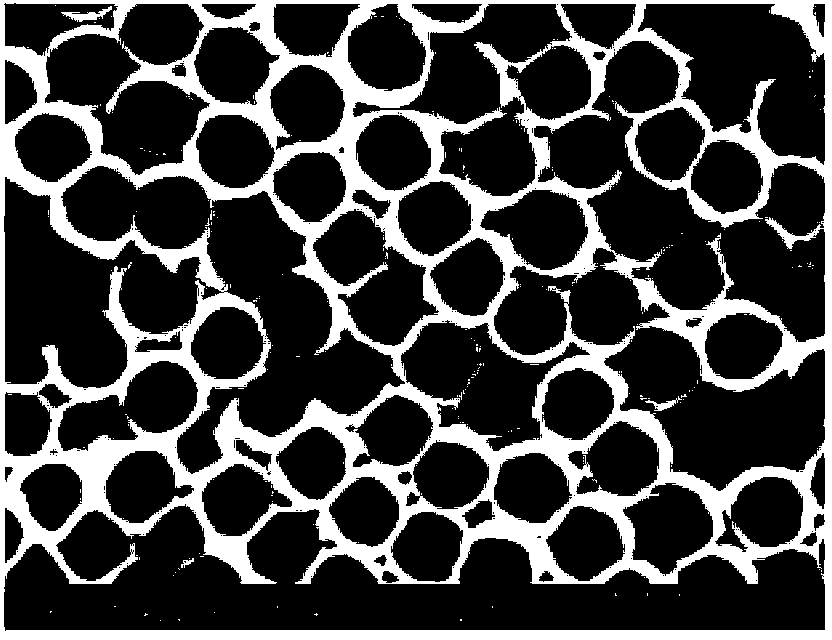
[0034] 0.5g NH 4 Dissolve F in 1mL water, stir well and add it into 49mL ethylene glycol and mix evenly to prepare bath A. Add the bath solution A into the electrolytic cell, use the cleaned titanium sheet as the anode, and the graphite electrode as the cathode, use a constant current stabilized power supply to apply a voltage of 20V to anodize for 0.5h, and then apply a voltage of 60V to anodize for 6h. Take it out and anneal it in a tube furnace at 500°C for 2h. Prepared TiO 2 nanotube array films, see figure 2 and 3 , it can be seen that the tube diameter is 100-150nm, the tube length is 4-80um, and the surface is smooth and highly ordered.

[0035] ②、TiO2 2 Fabrication of Nanotube Array Thin Film Mask

[0036] Dissolve 0.5ml of phenyltriethoxysilane into 48ml of methanol solution, slowly add 1.5ml of deionized water dropwise under slow stirring conditions, and continue stirring for 1h to prepare a phenyltr...

Embodiment 2

[0040] ①、TiO2 2 Fabrication of Nanotube Array Thin Films

[0041] 0.5g NH 4 Dissolve F in 1mL water, stir well and add it into 49mL ethylene glycol and mix evenly to prepare bath A. Add the bath solution A into the electrolytic cell, use the cleaned titanium sheet as the anode, and the graphite electrode as the cathode, use a constant current stabilized power supply to apply a voltage of 25V to anodize for 0.5h, and then apply a voltage of 70V to anodize for 5h. Take it out and anneal it in a tube furnace at 500°C for 2h.

[0042] ②、TiO2 2 Fabrication of Nanotube Array Thin Film Mask

[0043] Dissolve 0.5ml of phenyltriethoxysilane into 48ml of methanol solution, slowly add 1.5ml of deionized water dropwise under slow stirring conditions, and continue stirring for 2h to prepare a phenyltriethoxysilane-methanol composite solution. TiO prepared in step ① 2 The nanotube array thin film was put into the composite solution of phenyltriethoxysilane and methanol, and stirred sl...

Embodiment 3

[0047] ①、TiO2 2 Fabrication of Nanotube Array Thin Films

[0048] 0.6g NH 4 Dissolve F in 1mL water, stir well and add it into 49mL ethylene glycol and mix evenly to prepare bath A. Add the bath solution A into the electrolytic cell, use the cleaned titanium sheet as the anode, and the graphite electrode as the cathode, use a constant-current stabilized power supply to apply a voltage of 30V for anodization for 1h, and then apply a voltage of 80V for anodization for 4h. Take it out and anneal it in a tube furnace at 500°C for 2h.

[0049] ②、TiO2 2 Fabrication of Nanotube Array Thin Film Mask

[0050] Dissolve 0.5ml of phenyltriethoxysilane into 48ml of methanol solution, slowly add 1.5ml of deionized water dropwise under slow stirring conditions, and continue stirring for 2h to prepare a phenyltriethoxysilane-methanol composite solution. TiO prepared in step ① 2 The nanotube array thin film was put into the composite solution of phenyltriethoxysilane and methanol, and st...


PUM

PropertyMeasurementUnit
crystal sizeaaaaaaaaaa

Abstract

The invention belongs to the field of photoelectric nano-material technologies, and more specifically relates to a method used for preparing TiO2/Cu2O nano heterojunction by composite mask method. The method comprises following steps: titanium sheets are subjected to secondary anodic oxidation so as to obtain TiO2 nanotube array thin films; the TiO2 nanotube array thin films are immersed in a compound solution of phenyltriethoxysilane and methanol, and the TiO2 nanotube array thin films with super-hydrophobicity are prepared by mask method and ultraviolet light treatment; and then Cu2O nanocrystals produced by the high-frequency impulse electrodeposition method are uniformly distributed on the surface and inner wall of the TiO2 nanotube array thin films to obtain the TiO2/Cu2O nano heterojunction. The photoelectric property of the TiO2/Cu2O nano heterojunction is higher than 6 to 14 times of the photoelectric property of the TiO2 nanotube array; the photoelectric property is excellent; and the TiO2/Cu2O nano heterojunction can be used as ideal materials for solar energy photoelectric conversion and solar energy efficient utilization.

Description

technical field [0001] The invention relates to the technical field of optoelectronic nanomaterials, in particular to a compound mask method for preparing TiO 2 / Cu 2 O nanoheterojunction. Background technique [0002] TiO 2 It has unique advantages such as stable chemical properties, wide application range, non-toxicity, high catalytic activity, and strong oxidation ability, making it an excellent semiconductor material for photocatalysis. TiO 2 Nanotube array films have more 2 The more excellent photoelectric performance of the material is considered to be an ideal material for solar photoelectric conversion and efficient utilization of solar energy. [0003] However, TiO 2 There are two main problems in the application of nanotube array films: first, due to its wide band gap (about 3.2eV), it only absorbs light in the ultraviolet region, which greatly limits its practical application in sunlight; 1. Since the photogenerated carriers are easy to recombine, the utili...

Claims


Application Information

Patent Timeline
Patent Type & Authority Applications(China)
IPC IPC(8): C25D5/00C25D11/26C25D5/18B82Y40/00
Inventor 舒霞吴玉程沈天阔王岩
Owner HEFEI UNIV OF TECH
Why Eureka
Try Eureka