Supercharge Your Innovation With Domain-Expert AI Agents!

Composite substrate with isolation layer and manufacturing method thereof

A composite substrate and manufacturing method technology, applied in chemical instruments and methods, semiconductor/solid-state device manufacturing, crystal growth and other directions, can solve the problems of difficulty in forming a lattice structure, poor environmental protection, and complicated preparation methods for silicon SOI substrates, etc. Achieve the effect of improving performance and reducing production costs

Active Publication Date: 2015-07-22
INST OF PHYSICS - CHINESE ACAD OF SCI
View PDF6 Cites 0 Cited by
  • Summary
  • Abstract
  • Description
  • Claims
  • Application Information

AI Technical Summary

Problems solved by technology

[0005] The preparation method of the conventional silicon SOI substrate is relatively complicated, the process is difficult, the cost is high, and the environmental protection is poor. (bonding) process and another silicon wafer bond, and then thinning one of the silicon wafers through a thinning process to prepare an SOI substrate
[0006] The reason why the complex "bonding process" is usually used in the prior art is that the SOI substrate with the insulating isolation layer cannot be formed by successively growing the isolation layer and the semiconductor layer on the substrate by means of multi-layer continuous growth.
This is because the insulating isolation layer is usually amorphous, so it is difficult for the subsequent growth of the silicon semiconductor epitaxial layer to form a complete lattice structure

Method used


Image

  • Composite substrate with isolation layer and manufacturing method thereof
  • Composite substrate with isolation layer and manufacturing method thereof
  • Composite substrate with isolation layer and manufacturing method thereof

Examples


Embodiment 1

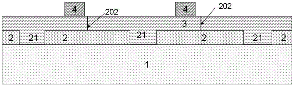
[0033] This embodiment provides a method for manufacturing a silicon SOI substrate with an insulating isolation layer, and its process flow is as follows Figure 1-7 shown, including:

[0034] 1) if figure 1 As shown, a 300nm thick SiO is formed on the surface of the silicon substrate 1 by thermal oxidation. 2 Thin film is used as the first sub-isolating layer 2, and then a plurality of openings 21 are formed in the first sub-isolating layer 2 by photolithography and etching processes, exposing the surface of the silicon substrate 1, and the plurality of openings 21 form a grating pattern, and its period is 4 microns, the width of the opening 21 is 1 micron;

[0035] 2) if figure 2 As shown, using the CVD lateral epitaxial growth technology, the silicon substrate 1 exposed at the opening 21 is used as a seed to prepare a silicon thin film as a seed layer 3, and the seed layer 3 starts epitaxial growth from the silicon substrate 1 at a plurality of openings 21, Then later...


PUM


Abstract

A manufacturing method of a composite substrate with an isolation layer comprises: 1) forming, on a silicon substrate, a first sub isolation layer with openings that expose the silicon substrate; 2) forming, on the first sub isolation layer and the silicon substrate by using a lateral growth method, a seed layer made of a silicon film; 3) forming a mask on the seed layer and covering a part of seed layer between the openings; 4) performing thermal oxidation on the seed layer to form a silicon dioxide layer, to use the silicon dioxide layer as a second sub isolation layer, a melting point of the mask being higher than a temperature in thermal oxidation on the seed layer; 5) removing the mask, and exposing the part of seed layer covered by the mask, to use the part of seed layer as a seed area.

Description

technical field [0001] The invention relates to a substrate for manufacturing semiconductor devices, in particular to a composite substrate with an isolation layer and a manufacturing method thereof. Background technique [0002] In the semiconductor industry, silicon materials are usually used as substrates, and various semiconductor devices are fabricated on silicon substrates by means of doping, photolithography, deposition, etc. The substrates are electrically coupled, resulting in large leakage currents, high power dissipation, and large parasitic capacitances. [0003] In recent years, a new semiconductor device substrate - silicon on insulator wafer (SOI, Silicon On Insulator) has been developed, which is composed of single crystal silicon on the top layer, silicon oxide on the insulator in the middle layer and single crystal silicon on the bottom layer , forming semiconductor devices in the top layer of single crystal silicon. SOI uses a silicon oxide insulating la...

Claims


Application Information

Patent Timeline
Patent Type & Authority Patents(China)
IPC IPC(8): H01L21/762H01L21/02H01L29/06
CPCC30B29/06C30B25/04C30B25/183H01L21/7624
Inventor 陈弘贾海强江洋王文新马紫光王禄李卫
Owner INST OF PHYSICS - CHINESE ACAD OF SCI
Features
  • R&D
  • Intellectual Property
  • Life Sciences
  • Materials
  • Tech Scout
  • Unparalleled Data Quality
  • Higher Quality Content
  • 60% Fewer Hallucinations
Learn More