

Crystalline silicon solar cell resisting to PID effect and manufacturing method thereof
A solar cell, crystalline silicon technology, applied in circuits, electrical components, semiconductor devices, etc., can solve the problems of poor adhesion between silicon nitride and silicon materials, PID attenuation, and component output power drop, etc., to enhance the passivation effect, Improves performance and prevents contamination
- Summary
- Abstract
- Description
- Claims
- Application Information
AI Technical Summary
Problems solved by technology
Method used
Image

Examples
Embodiment 1
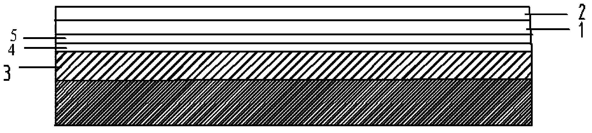
[0018] A kind of anti-PID effect crystalline silicon solar cell of the present invention, its structure diagram is as follows figure 1 As shown, it includes a silicon substrate and a passivation film arranged on the silicon substrate, and the passivation film includes a dense layer of SiO deposited on the front surface of the silicon substrate in sequence. 2 , loose layer SiO 2 , dense layer Si 3 N 4 and loose layer Si 3 N 4 .
[0019] The dense layer of SiO 2 Thickness is 5nm, the loose layer SiO 2 The thickness is 10nm; the dense layer Si 3 N 4 The refractive index of 2.3, thickness is 10nm; The loose layer Si 3 N 4 The refractive index is 2.08 and the thickness is 60nm.
[0020] The preparation method of the anti-PID effect crystalline silicon solar cell: including texturing-diffusion-etching-oxidation-PECVD-screen printing-sintering test steps, oxidation and PECVD steps are:
[0021] (1) On the etched silicon wafer substrate, a dense layer of SiO is formed by h...
Embodiment 2
[0024] The dense layer SiO in embodiment 1 2 Thickness processing is 7nm, loose layer SiO 2 Thickness processing is 13nm, dense layer Si 3 N 4 Thickness processing is 13nm, dense layer Si 3 N 4 Refractive index 2.33, loose layer Si 3 N 4 Thickness processing is 63nm, loose layer Si 3 N 4 The refractive index is 2.09, and other main process parameters remain unchanged, so that a crystalline silicon solar cell resistant to PID effect is produced.
Embodiment 3
[0026] The dense layer SiO in embodiment 1 2 Thickness processing is 8nm, loose layer SiO 2 Thickness processing is 15nm, dense layer Si 3 N 4 Thickness processing is 15nm, dense layer Si 3 N 4 Refractive index 2.35, loose layer Si 3 N 4 Thickness processing is 65nm, loose layer Si 3 N 4 The refractive index is 2.10, and other main process parameters remain unchanged, so that a crystalline silicon solar cell resistant to PID effect is produced.
PUM
 Abstract
Description
Claims
Application Information