
Polycrystalline silicon and preparation method thereof

A technology of polysilicon and silicon materials, applied in the field of solar cells, can solve the problems of not adopting large-scale production, high input cost, and low material yield, and achieve the effects of less dislocation defects, high material yield, and simple operation

Inactive Publication Date: 2013-12-04
HUNAN RED SUN PHOTOELECTRICITY SCI & TECH
View PDF8 Cites 12 Cited by
  • Summary
  • Abstract
  • Description
  • Claims
  • Application Information

AI Technical Summary

Problems solved by technology

[0005] However, the input cost of the above-mentioned first method is relatively high, and it is basically not used in large-scale production.
The second method is widely used at present, but the operation of this method is complicated, and the operator needs to have skilled operation experience to ensure that the seed crystal at the bottom of the crucible is not completely melted, and the yield is not high.

Method used


Image

  • Polycrystalline silicon and preparation method thereof
  • Polycrystalline silicon and preparation method thereof

Examples


Embodiment 1

[0026] Prepare a quartz crucible whose bottom inner surface is rough and sprayed with quartz sand, and prepare an ingot furnace. The model of the ingot furnace is R13800-1 / UM.

[0027] The preparation method of the polysilicon includes the following steps:

[0028] (1) Put 810 kg of silicon material doped with electroactive dopants into a quartz crucible, the target resistivity of the silicon material doped with electroactive dopants is 1.7Ω·cm, and put the quartz crucible into the ingot furnace Vacuum and heat in the insulated cage;

[0029] (2) Control the temperature of the ingot furnace heater to 1560°C, then keep the heater temperature at 1560°C to completely melt the silicon material. When the silicon material is completely melted, control the temperature of the bottom of the quartz crucible to 1420°C;

[0030] (3) Reduce the temperature of the ingot furnace heater from 1560°C to 1425°C with a temperature drop rate of 150-200°C / h, and then keep it for 30-90 minutes;

[0031] (4) ...


PUM


Abstract

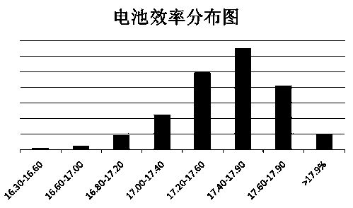
The invention discloses a preparation method of polycrystalline silicon. According to the method, the twin crystal growth control technology is adopted, the ordinary polycrystalline process is optimized, a heat insulation cage is quickly opened, and the opening of the heat insulation cage is adjusted to be 6-8cm; at the initial stage of growth of the crystal, the temperature of a heater is adjusted to be 1425-1440 DEG C, the heat insulation cage is slowly lifted, a layer of uniform dendritic crystal grows vertically on a nucleation source layer along the bottom of a crucible, then dendritic crystal is taken as the seed crystal, and vertically upward directionally grows to form the polycrystalline silicon. The polycrystalline silicon prepared by the invention contains a great quantity of twin crystals, as the twin crystals have the advantages that the interfacial energy of the twin crystals is low, the twin crystals are relatively more stable, and the like, and the polycrystalline silicon prepared by the method has the advantage of few dislocation defects, the battery efficiency of the polycrystalline silicon is higher than that of the ordinary polycrystalline silicon for 0.2-0.4%, the average battery efficiency of a whole silicon wafer reaches 17.5%, and the highest efficiency reaches 18.0%.

Description

technical field [0001] The invention belongs to the technical field of solar cells, and in particular relates to a method for preparing polysilicon. Background technique [0002] Crystalline silicon is the most commonly used semiconductor material in the manufacture of solar cells. At present, the crystalline silicon used in the manufacture of solar cells is mainly monocrystalline silicon by Czochralski method and polycrystalline silicon by ingot casting technology. Polysilicon ingot casting has a large amount of feeding, simple operation, and low process cost, but low conversion efficiency and short life of the battery; Czochralski monocrystalline silicon has high conversion efficiency, but less single feeding, complicated operation, and high cost, so it is basically eliminated. [0003] High-efficiency polysilicon ingot preparation technology can be said to be the development of the second-generation ingot technology. The nucleation and growth of silicon crystals are con...

Claims


Application Information

Patent Timeline
Patent Type & Authority Applications(China)
IPC IPC(8): C30B28/06C30B29/06
Inventor 谭晓松段金刚
Owner HUNAN RED SUN PHOTOELECTRICITY SCI & TECH
Learn More