Method for measuring graphic density

A pattern density and pattern technology, which is applied in the photoplate making process of the pattern surface, semiconductor/solid-state device testing/measurement, and original parts for photomechanical processing, etc., can solve the problem of large setting errors of etching and grinding process parameters, Problems such as the large difference between the measured pattern density and the actual pattern density can achieve the effect of improving yield and supporting accurate data

Active Publication Date: 2013-12-11
SHANGHAI HUALI MICROELECTRONICS CORP
View PDF6 Cites 8 Cited by
  • Summary
  • Abstract
  • Description
  • Claims
  • Application Information

AI Technical Summary

Problems solved by technology

[0012] In view of the above-mentioned existing problems, the present invention provides a method for measuring pattern density, to overcome the problem of large difference between measured pattern density and actual pattern density in the prior art because there is no effective method for testing pattern density, and also overcomes the problem of In the prior

Method used


Image

  • Method for measuring graphic density
  • Method for measuring graphic density
  • Method for measuring graphic density

Examples


Embodiment 1

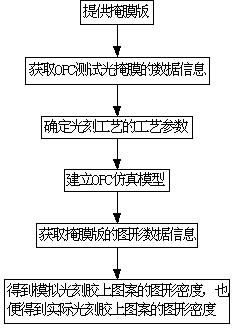
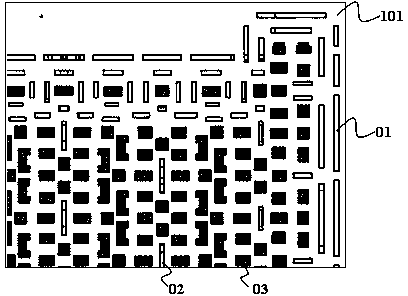
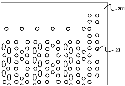
[0043] figure 1 It is a schematic flow chart of the method for measuring pattern density provided by Embodiment 1 of the present invention; figure 2 It is a schematic diagram of the mask pattern to be tested provided by Embodiment 1 of the present invention; image 3 It is a schematic diagram of simulating the pattern on the photoresist provided by Embodiment 1 of the present invention; as shown in the figure, the method for measuring the pattern density is mainly used in the process of measuring the pattern density of the pattern on the photoresist, including the following steps:

[0044]First, according to the process requirements, that is, according to the products required by customers, a test photolithography mask plate with a pattern of multiple OPC test photomasks is provided. At the same time, the mask plate includes all Graphics that may appear.

[0045] Then obtain the data information of the OPC test photomask. The specific operation is: transfer the pattern of t...


PUM


Abstract

The invention discloses a method for measuring graphic density. An OPC (optical proximity correction) simulation model is constructed through a lithography process simulation module supplied by OPC software by acquiring data information of an OPC test photomask and technical parameter information of a lithography technology; the graph of a mask to be tested is introduced into the constructed OPC simulation model, so that patterns of the mask to be tested formed on photoresist can be simulated, and the graphic area of the patterns on the photoresist can be simulated; furthermore, the graphic density of the simulated patterns formed on the photoresist can be obtained, namely the graphic density of actual patterns formed on the photoresist is obtained. According to a simulation method, the graphic density of the patterns on the photoresist can be precisely obtained, so that the problem that the measured graphic density is greatly different from the actual graphic density because of no effective method for measuring the graphic density in the prior art is solved, and the graphic density is accurately measured; accurate data support is supplied to the subsequent manufacture procedure development such as etching and grinding, and the yield of a product is further improved.

Description

[0001] technical field [0002] The invention relates to the technical field of semiconductor testing, in particular to a method for measuring pattern density. [0003] Background technique [0004] With the continuous improvement of integrated circuit process technology, especially after the 0.13 micron process, the line width of the silicon process is already smaller than the wavelength length of exposure, making process stability more and more difficult. The derivative effects of the process are considered in the early stage of design, resulting in a lot of design rule checks (DRC, Design Rule Check). Design rule checking includes many aspects, among which the overall and local pattern density (Pattern Density) has a great influence on chemical mechanical polishing (CMP, Chemical Mechanical Polarization) and etching macro loading (Macro Loading). [0005] In the prior art, the pattern density on the photoresist is usually obtained by measuring the pattern density of the...

Claims


Application Information

Patent Timeline
IPC IPC(8): G03F7/20G03F1/36G03F1/44H01L21/66
Inventor 王丹于世瑞孙贤波
Owner SHANGHAI HUALI MICROELECTRONICS CORP
Why Eureka
Try Eureka