SiC optical material processing device

A technology for processing equipment and optical materials, applied in electrical components, semiconductor/solid-state device manufacturing, circuits, etc., can solve the problems of difficult to guarantee product quality and processing cycle, low processing efficiency, sub-surface damage, etc., to achieve simple structure, processing The effect of increased speed and low cost

Active Publication Date: 2013-12-18
NAT UNIV OF DEFENSE TECH
View PDF4 Cites 5 Cited by
  • Summary
  • Abstract
  • Description
  • Claims
  • Application Information

AI Technical Summary

Problems solved by technology

[0005] Traditional lapping and polishing methods are suitable for small and single-piece processing of SiC optical materials. Combining manual repair and polishing can also solve the processing problems of some aspheric surfaces, but the processing efficiency is low, the accuracy convergence is slow, and product quality and processing cycle are not easy to guarantee.
[0006] The grinding method has a high material removal rate, but subsurface damage occurs during the grinding process, and at the same time, a residual stress layer is formed on the surface of the workpiece
[0007] The computer-controlled deterministic polishing method is the key technology for obtaining higher surface accuracy. The methods that can be used to process SiC optical materials mainly include dual-rotor small tool polishing method, ion beam modification method and magnetorheological polishing method. However, The processing efficiency of the above method is low

Method used


Image

  • SiC optical material processing device
  • SiC optical material processing device
  • SiC optical material processing device

Examples


Embodiment Construction

[0031] The present invention will be described in further detail below in conjunction with the accompanying drawings and specific embodiments.

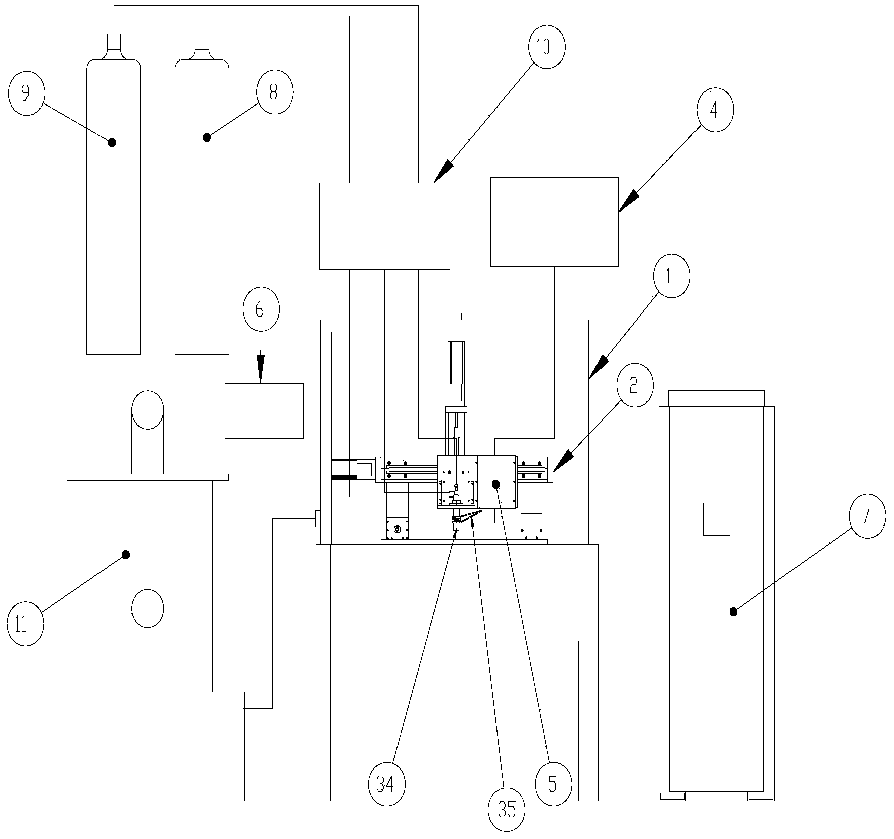
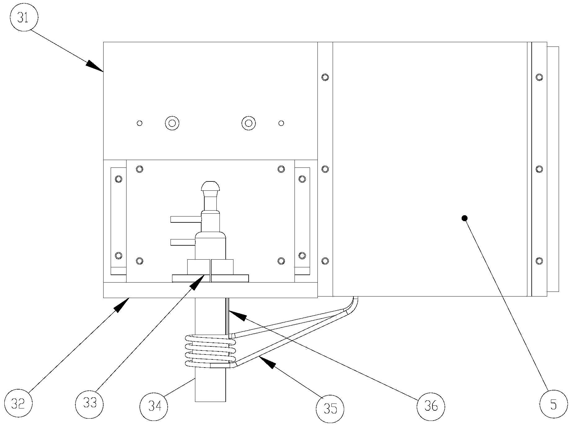
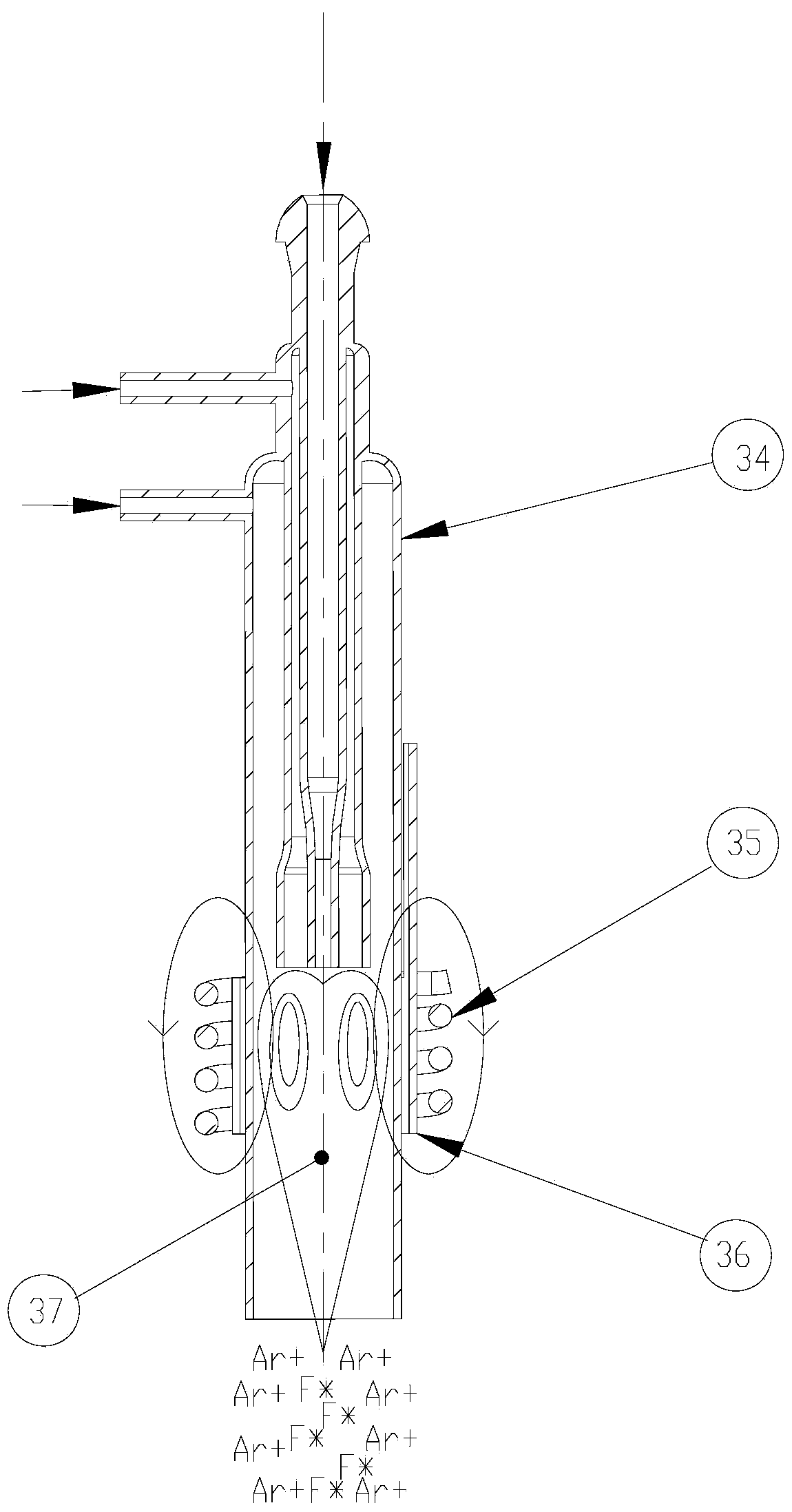
[0032] Such as figure 1 As shown, the SiC optical material processing equipment of the present invention includes an inductively coupled plasma generator, a working gas supply source 8 and a reactive gas supply source 9, and the reactive gas supply source 9 is equipped with a Reactive gases that chemically react with SiC, such as SF 6 or NF 3 or CF 4 . The inductively coupled plasma generating device includes a plasma torch 34 and an induction coil 35 sleeved outside the plasma torch 34, and the plasma torch 34 is used to generate a plasma torch 37 (see image 3 ), the plasma torch 34 uses a Fassel torch, which is widely used in ICP-OES spectrometer equipment, with low cost and mature technology, and can be used to generate stable plasma and excite reaction gases. Wherein, the working gas supply source 8 is connected with the mid...


PUM


Abstract

The invention discloses an SiC optical material processing device which comprises an inductive coupling plasma generation device, a working gas supply source (8) and a reaction gas supply source (9). Reaction gas which can have chemical reaction with SiC after being stimulated by the inductive coupling plasma generation device is placed in the reaction gas supply source (9), the inductive coupling plasma generation device comprises a plasma torch pipe (34) and an induction coil (35), the plasma torch pipe (34) is sleeved with the induction coil (35), the working gas supply source (8) and the reaction gas supply source (9) are connected with the plasma torch pipe (34), one end of the induction coil (35) is connected with a radio-frequency power source (4), and the other end of the induction coil (35) is grounded through an adjustable resistor R1. The SiC optical material processing device has the advantages of being simple in structure and low in cost, producing no subsurface damage or residual stress in a processing procedure, having high processing efficiency and the like.

Description

technical field [0001] The invention mainly relates to the field of optical material processing equipment, in particular to a SiC optical material processing equipment. Background technique [0002] With the rapid development of space astronomical optics, satellite remote sensing technology, and large-scale ground-based optical systems, the requirements for the operating band, imaging resolution, thermal stability, and system weight of the optical system are becoming more and more stringent. Therefore, the optical system is moving along the Reflective, large-diameter, and lightweight trends develop. In optical system design, selecting the appropriate reflector material is of great significance to meet the above indicators. Due to the constraints of difficult manufacturing, high launch and operating costs, and special working environment in space optical systems, the following aspects must be considered in the selection of space mirror materials: (1) Isotropic and dimensiona...

Claims


Application Information

Patent Timeline
Patent Type & Authority Applications(China)
IPC IPC(8): H01L21/263G02B5/08
Inventor 解旭辉史宝鲁李圣怡戴一帆周林廖春德
Owner NAT UNIV OF DEFENSE TECH
Why Eureka
Try Eureka