

High-power overload 1KPa silicon micropressure sensor chip and manufacturing method
A technology of a pressure sensor and a manufacturing method, applied in the field of high overload 1KPa silicon micro-pressure sensor chip and manufacturing, can solve the problems such as the batch manufacturing process of the silicon piezoresistive pressure sensor micro-pressure sensor, which is easy to implement and cost. low effect
- Summary
- Abstract
- Description
- Claims
- Application Information
AI Technical Summary
Problems solved by technology
Method used
Image

Examples
Embodiment Construction
[0027] Below in conjunction with accompanying drawing and embodiment the present invention will be further described:
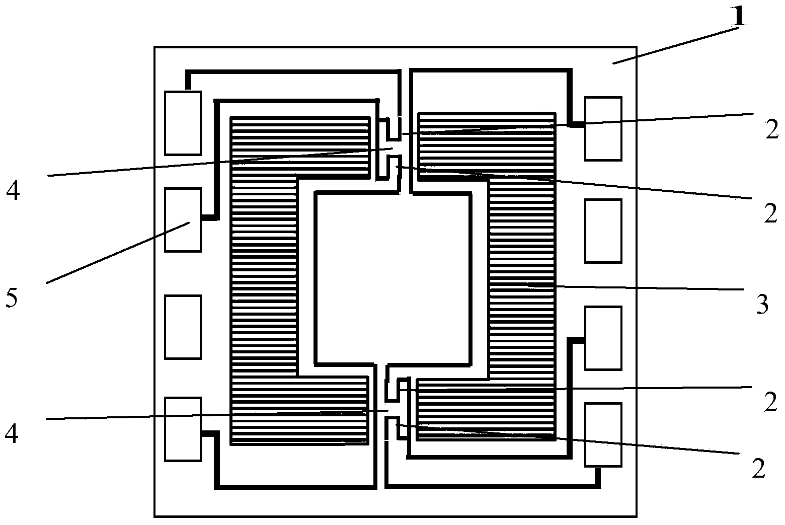
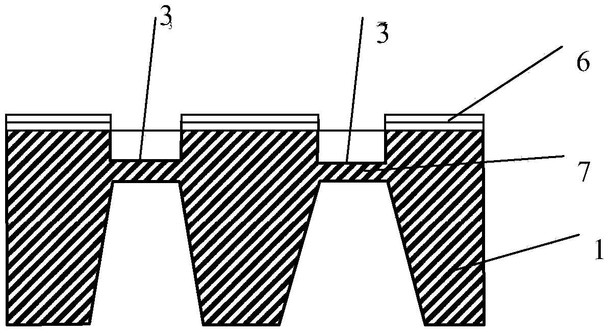
[0028]The high-magnification overload 1KPa silicon micro-pressure sensor chip manufactured by the method of the present invention adopts a 4-inch double-sided polished silicon single wafer, which is characterized in that the structural feature: the microstructure processed on both sides of the upper chip 1: the front "I" beam structure, single rigid membrane structure on the back; see figure 1 , the "back"-shaped shallow groove 3 formed by the corrosion of the upper chip 1, leaving two "I"-shaped beams 4, symmetrically separating the "back" character, and each of the "I"-shaped beams 4 has two single elbows "U" Shaped pressure sensitive resistor, the shallow groove 3 is surrounded by aluminum electrode leads and lead pads 5 . On the back of the upper chip 1, the material other than the thickness of the diaphragm is processed relative to the shallow groove 3,...
PUM
| Property | Measurement | Unit |
|---|---|---|
| Thickness | aaaaa | aaaaa |
| Resistivity | aaaaa | aaaaa |
| Thickness | aaaaa | aaaaa |
Abstract
Description
Claims
Application Information