Method and electrode structure for improving microelectrode array electrode density based on electrochemical bipolar behavior

A micro-electrode array and micro-electrode technology, applied in the field of micro-electrode array electrochemistry, to achieve the effects of simple experimental equipment, increased density, and enhanced current response

Inactive Publication Date: 2014-01-01
XIAMEN UNIV
View PDF2 Cites 8 Cited by
  • Summary
  • Abstract
  • Description
  • Claims
  • Application Information

AI Technical Summary

Problems solved by technology

In this way, there is a positive feedback phenomenon between the needle tip and the substrate to which no potential is applied 12

Method used


Image

  • Method and electrode structure for improving microelectrode array electrode density based on electrochemical bipolar behavior
  • Method and electrode structure for improving microelectrode array electrode density based on electrochemical bipolar behavior
  • Method and electrode structure for improving microelectrode array electrode density based on electrochemical bipolar behavior

Examples


Embodiment 1

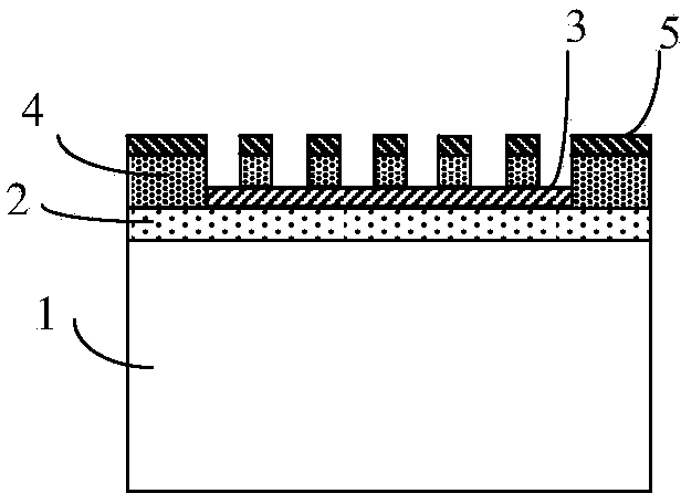
[0071] This embodiment adopts figure 1 The electrode configuration shown is carried out, the shape of the microelectrode is a disk electrode, the material of the microdisk electrode (the first layer of metal material) is Au, the plane metal film (the second layer of metal material) is also Au, and the insulating material is polymer Polyimide (PI). The parameters are designed as follows: the radius of the microdisk electrode is fixed at 6 μm, and a series of electrode arrays with electrode center-center spacing are designed for different units: d~6r, 8r, 10r, 12r, 15r, 20r, these microelectrodes are distributed in an area of ​​810 μm×810 μm On the gold film, combined with the viscosity, the thickness of the polyimide is about 2 μm by adjusting the speed of the homogenizer. The size of the planar gold film electrodes is 2mm. Figure 5a It is the scanning electron microscope image of the plane-concave microdisk electrode array at d~12r. In electrochemical experiments, with 5mM...

Embodiment 2

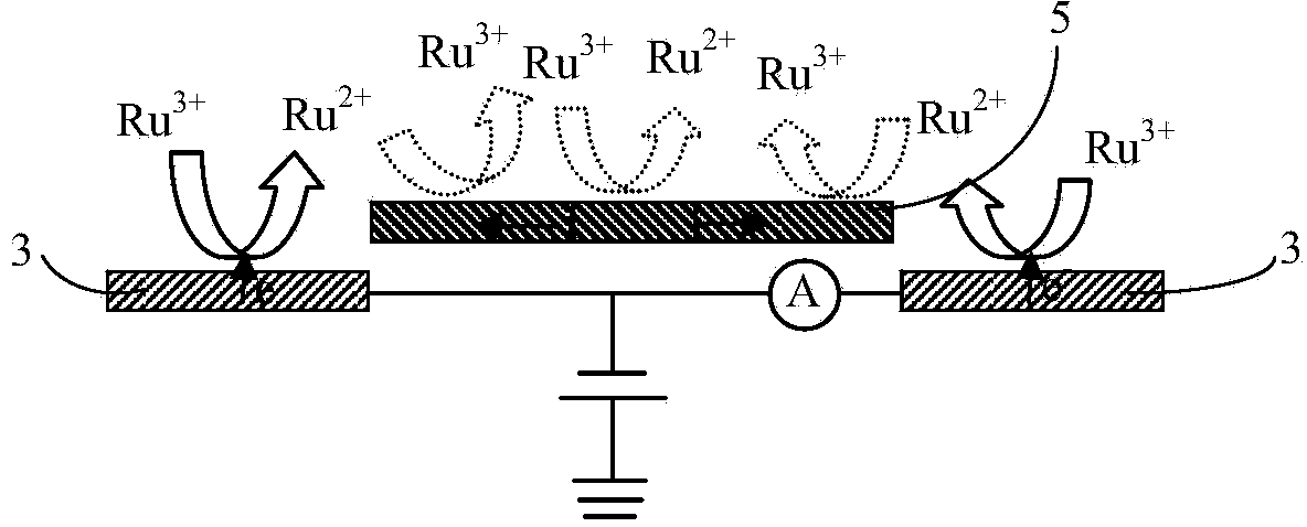
[0073] This embodiment adopts figure 1 The electrode configuration shown is carried out, the microdisk electrode material is Au, the plane metal film material is also Au, and the insulating layer is still polyimide (PI). The electrode parameters are as follows: the radius of the microdisk electrode is 6.8 μm, the number of fixed electrodes is an array of 5×5, the electrode spacing is changed from d to 4r, 6r, 8r, 10r, 12r, the thickness of PI is 2.8 μm, and the plane metal film is a whole layer of Au . The scanning electron microscope picture at d~4r is as follows Figure 6a As shown, during the electrochemical experiment, ensure that the droplet passes through the concave microdisk electrode array. The electrochemical experiment process was the same as in Example 1. When the planar metal film is in an open circuit, the electrochemical CV of the concave microdisk electrode array is as follows: Figure 6b As shown, 1, 2, 3, and 4 correspond to the CVs when the electrode spa...


PUM

PropertyMeasurementUnit
thicknessaaaaaaaaaa
sizeaaaaaaaaaa
radiusaaaaaaaaaa

Abstract

The invention discloses a method and electrode structure for improving microelectrode array electrode density based on an electrochemical bipolar behavior, and belongs to the field of microelectrode array electrochemistry. In the study of a microelectrode array, the aim of how to design electrode spacing to enable the microelectrode array to maintain the property of microelectrode stability and meanwhile to achieve the sum of currents is always a hot point. The electrode structure, based on an electrochemical bipolar phenomenon, of a plane-concave microelectrode array is provided, a plane metal film layer is introduced over the concave microelectrode array, the metal film covers the insulation layer of the concave microelectrode array, and microelectrodes are exposed. Therefore, the microelectrode array can still obtain the property of steady state responses under the condition of small electrode spacing, meanwhile, due to the microelectrode bipolar phenomenon, steady-state currents are larger than the steady-state currents of common electrodes, and therefore a large current response can be obtained on a small chip, and a current density value is increased by at least one magnitude order.

Description

technical field [0001] The invention belongs to the field of electrochemistry of microelectrode arrays, and relates to the design and processing of planar-concave microelectrode arrays, and the use of the electrochemical bipolar behavior of planar metal films to improve the integration of electrodes in the concave microelectrode arrays, thereby improving sensitivity. Planar-concave microelectrode arrays can be used as electrochemical sensors, for example to detect small organic molecules. Background technique [0002] A microelectrode is an electrode with at least one dimension below 25 μm. The radial diffusion caused by the edge effect makes the microelectrode have the characteristics of high current density, small charging current, fast response time, and high signal-to-noise ratio. However, the response of a single microelectrode is very small (~nA level), which limits the application of microelectrodes to a certain extent. The microelectrode array, as an ordered collect...

Claims


Application Information

Patent Timeline
Patent Type & Authority Applications(China)
IPC IPC(8): H01L21/02B81C1/00
CPCG01N27/30B81C1/00031
Inventor 朱凤颜佳伟毛秉伟
Owner XIAMEN UNIV
Why Eureka
Try Eureka