
Eureka
For R&D, Eureka makes reading and utilizing patents & technical documents easy.
Eureka AIR
Designed for self-driven R&D workflows. Generate viable solutions, solve complex R&D challenges, empower your innovation with AI.

Eureka Materials
Designed for material experts only. Revolutionize your material R&D, from search, analyze, to developing new materials.

TechResearch
Generate reliable direction feasibility study reports for your R&D in just a few steps.

TechSeek
Discover and master advanced knowledge NOW. Basics, ideas, possibilities, all at once.

TechMind
As an expert in R&D Theories, TechMind can generates customized viable solutions instantly.

TechRisk
Analyze your overall solution with one click, know your potential R&D risks in advance.

TechMonitor
Get weekly tech updates, stay abreast of the latest tech innovations and key insights.
Preparation method of low-temperature polysilicon thin film, thin film transistor and display device
A low-temperature polysilicon and amorphous silicon thin film technology, which is applied to transistors, electric solid-state devices, semiconductor devices, etc., can solve problems such as unfavorable low-temperature polysilicon thin film transistor performance, unfavorable low-temperature polysilicon thin film cost reduction, and difficulty in the preparation of low-temperature polysilicon thin films. , to achieve the effect of improving display effect, excellent electrical properties, and improving grain size and uniformity
- Summary
- Abstract
- Description
- Claims
- Application Information
AI Technical Summary
Problems solved by technology
Method used
Image

Examples
Embodiment Construction
[0039] The following will clearly and completely describe the technical solutions in the embodiments of the present invention with reference to the accompanying drawings in the embodiments of the present invention. Obviously, the described embodiments are some of the embodiments of the present invention, but not all of them. Based on the embodiments of the present invention, all other embodiments obtained by persons of ordinary skill in the art without making creative efforts belong to the protection scope of the present invention.
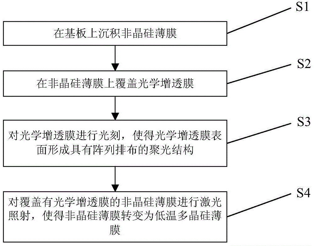
[0040] The embodiment of the present invention provides a method for preparing a low-temperature polysilicon thin film, such as figure 1 As shown, the method includes:
[0041] Step S1, depositing an amorphous silicon thin film on the substrate.
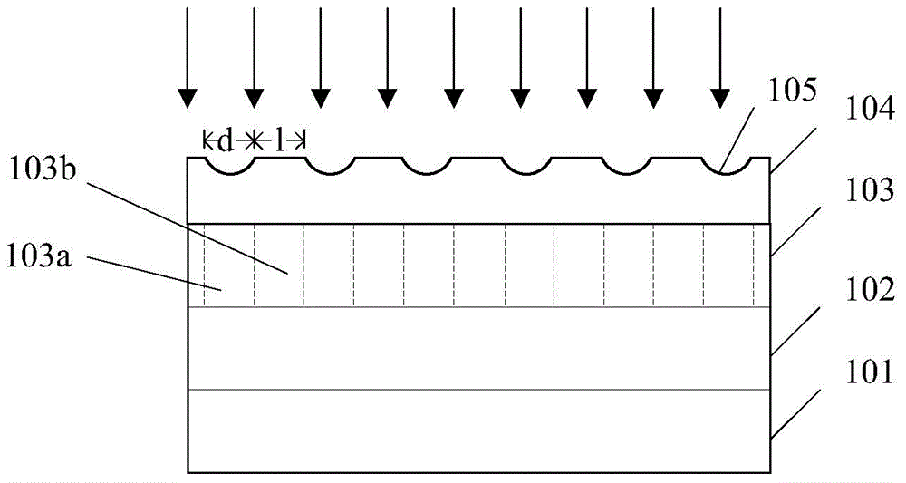
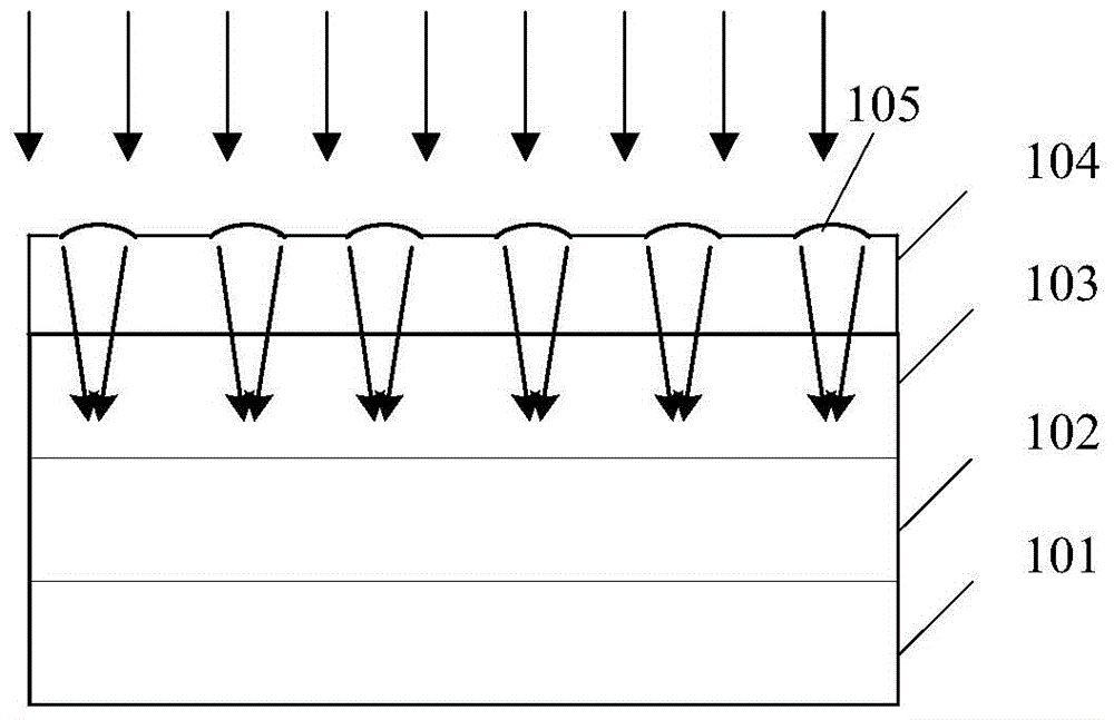
[0042] Preferably, as figure 2 As shown, before depositing the amorphous silicon film, a buffer layer 102 may also be deposited on the substrate 101, which may be silicon nitride or silicon oxide.
...
PUM
| Property | Measurement | Unit |
|---|---|---|
| diameter | aaaaa | aaaaa |
| diameter | aaaaa | aaaaa |
| thickness | aaaaa | aaaaa |
Abstract
Description
Claims
Application Information
 - R&D Engineer
- R&D Manager
- IP Professional
- Industry Leading Data Capabilities
- Powerful AI technology
- Patent DNA Extraction
Browse by: Latest US Patents, China's latest patents, Technical Efficacy Thesaurus, Application Domain, Technology Topic, Popular Technical Reports.
© 2024 PatSnap. All rights reserved.Legal|Privacy policy|Modern Slavery Act Transparency Statement|Sitemap|About US| Contact US: help@patsnap.com