LED based on photonic crystal-single-layer graphene structure

A single-layer graphene and photonic crystal technology, used in semiconductor devices, electrical components, circuits, etc., can solve problems such as expensive, high preparation temperature, lack of flexibility, etc., to reduce high costs, improve heat dissipation, and improve light extraction efficiency. Effect

Inactive Publication Date: 2014-01-01
BEIJING UNIV OF TECH
View PDF3 Cites 7 Cited by
  • Summary
  • Abstract
  • Description
  • Claims
  • Application Information

AI Technical Summary

Problems solved by technology

[0004] In traditional GaN-LEDs, indium tin oxide (ITO) is the most widely used transparent electrode material as the transparent conductive layer, but the preparation temperature is high and expensive, mainly because it needs to grow scarce indium on the surface, and the price of indium is high and supply is limited
The ITO material is relatively brittle and lacks flexibility, which makes it unable to meet the performance requirements of some new applications (such as bendable), and the cost of deposition in vacuum is relatively high in the fabrication of electrode engineering, and the light transmittance of ITO is only 90%.

Method used


Image

  • LED based on photonic crystal-single-layer graphene structure
  • LED based on photonic crystal-single-layer graphene structure
  • LED based on photonic crystal-single-layer graphene structure

Examples


Embodiment Construction

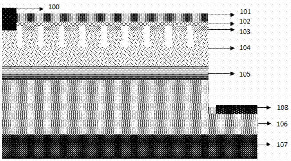
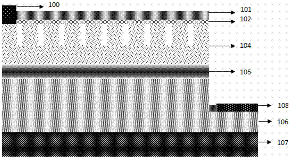
[0033] LEDs based on photonic crystal-single-layer graphene structures such as figure 1 Shown, wherein the preparation method process can be found in Figure 4 . First, a 1 nm thick contact layer is deposited on p-GaN using electron beam evaporation.

[0034] Use inductively coupled plasma etching (ICP) to carve the negative electrode part, with a depth of 1.2um.

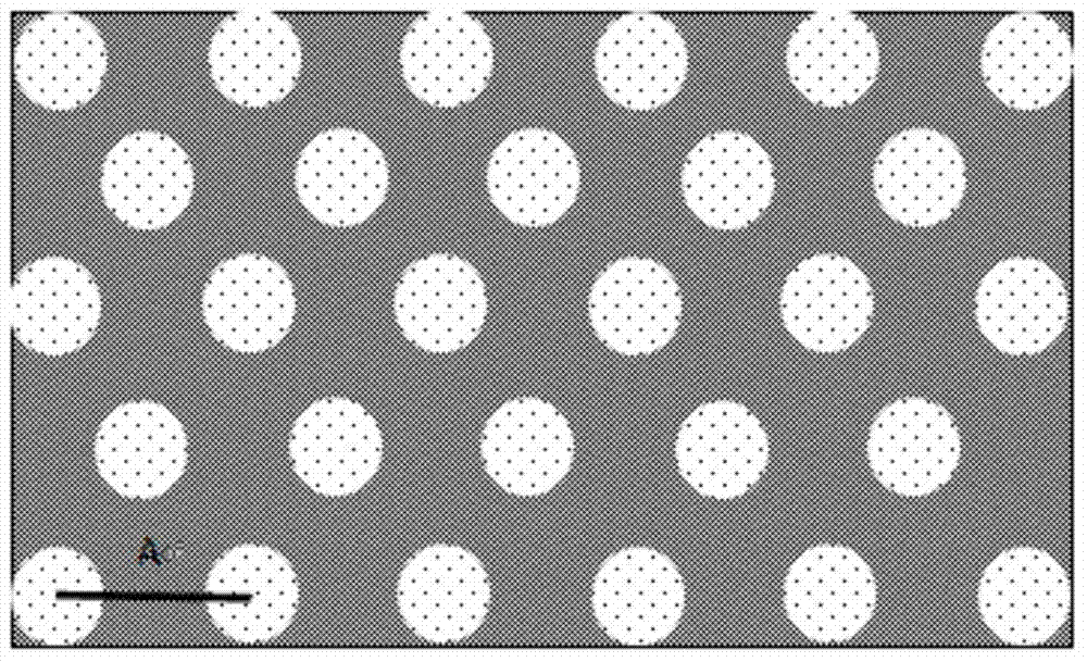
[0035] The photonic crystal structure was fabricated by inductively coupled plasma etching (ICP) in the p-GaN counterpart, see image 3 , the distance between adjacent circle centers is A=460nm, the radius of the circle is r=210nm, and the depth of the circular hole is h=120nm.

[0036] Transfer of single-layer graphene onto LEDs.

[0037] Sputtered titanium gold electrode (50nm).

[0038] A protective layer of silicon dioxide (300nm) was deposited by PECVD.

[0039] Compared with traditional GaN-LEDs, the light extraction efficiency of the present invention can be increased by more than 40%.

[0040] Above,...


PUM


Abstract

The invention discloses an LED based on a photonic crystal-single-layer graphene structure, and belongs to the technical field of LEDs. The LED sequentially comprises a silicon dioxide protective layer, monoatomic-layer graphene, a contact layer (not essential), an LED chip p-GaN layer, an LED chip multi-quantum well light emitting layer, an LED chip n-GaN layer and a sapphire substrate from top to bottom, wherein the LED chip p-GaN layer is of a photonic crystal structure, and the protective layer covers all the portions except for a positive electrode and a negative electrode. The structure of combining the photonic crystal and the single-layer graphene is adopted, so that the aim of greatly improving the light emitting efficiency and being free of using an ITO at the same time is achieved.

Description

technical field [0001] The invention is an LED based on a photonic crystal-single-layer graphene structure, relates to an LED structure capable of greatly improving light extraction efficiency, and belongs to the technical field of LEDs. technical background [0002] With the continuous development of LED technology, LED is more and more used in the field of lighting and display. As a lighting source, LED has the advantages of environmental protection and energy saving compared with traditional light sources. The potential and advantages of LED replacing incandescent lamps and fluorescent lamps as the next generation of lighting sources are becoming more and more obvious. In recent years, as the core part of making white LEDs, GaN-LEDs have played an extremely important role in the demand for high-brightness and multi-color LEDs. LED is an ideal lighting device with higher brightness and lower energy consumption required by future social development. Due to the limitation ...

Claims


Application Information

Patent Timeline
Patent Type & Authority Applications(China)
IPC IPC(8): H01L33/40
CPCH01L33/44
Inventor 徐晨葛海亮许坤郑雷陈茂兴
Owner BEIJING UNIV OF TECH
Why Eureka
Try Eureka