Production method of 50-micron ultrathin chips

A production method and technology for ultra-thin chips, applied in electrical components, semiconductor/solid-state device manufacturing, circuits, etc., to reduce resistance, reduce chip cracks and chipping, and ensure processing capabilities.

Active Publication Date: 2014-01-15
TIANSHUI HUATIAN TECH +1
View PDF3 Cites 27 Cited by
  • Summary
  • Abstract
  • Description
  • Claims
  • Application Information

AI Technical Summary

Problems solved by technology

[0004] The purpose of the present invention is to provide a 50 μm ultra-thin chip production method, which is used to produce ultra-thin chips, provides guarantee for ultra-thin laminated chip packaging, meets the developm

Method used


Image

  • Production method of 50-micron ultrathin chips
  • Production method of 50-micron ultrathin chips
  • Production method of 50-micron ultrathin chips

Examples


Embodiment 1

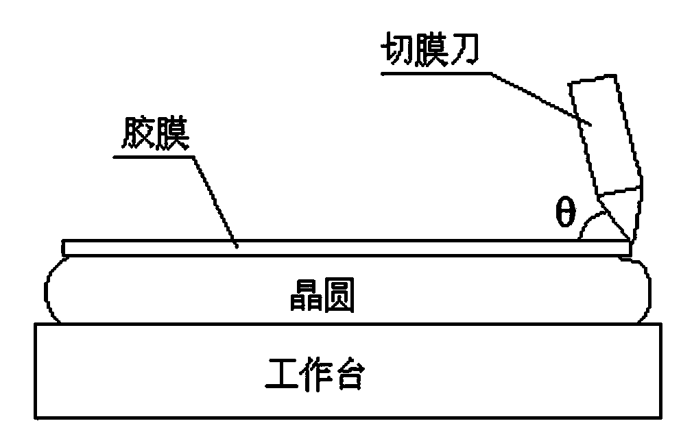
[0048] Paste semiconductor-specific UV adhesive film on the surface of the wafer graphics; according to the shape of the wafer positioning edge, set the corresponding blade running track parameters and film cutting speed to ensure that the running track of the film cutting blade changes with the different positioning sides, and the whole After cutting the wafer, the film cutting track matches the shape of the wafer edge. The cutting speed of the film cutting is 10mm / sec. When the number of film (wafer) cut by the film cutting knife reaches 1000pcs, replace the film cutting knife; the film cutting knife between the film cutting knife and the wafer surface when cutting the film The angle θ is 65°; a fully automatic thinning machine capable of thinning 12-inch ultra-thin wafers (50μm) is adopted. First, automatic feeding, positioning, and then thinning. The thinning process is divided into three stages. First coarse grinding, then fine grinding;

[0049]The rough grinding range ...

Embodiment 2

[0051] Paste semiconductor-specific UV adhesive film on the surface of the wafer graphics; according to the shape of the wafer positioning edge, set the corresponding blade running track parameters and film cutting speed to ensure that the running track of the film cutting blade changes with the different positioning sides, and the whole After cutting the wafer, the film cutting track matches the shape of the wafer edge. The cutting speed of the film cutting is 30mm / sec. When the number of film (wafer) cut by the film cutting knife reaches 1000pcs, replace the film cutting knife; the film cutting knife between the film cutting knife and the wafer surface when cutting the film The angle θ is 90°; a fully automatic thinning machine capable of thinning 12-inch ultra-thin wafers (50μm) is adopted. First, the material is automatically loaded, positioned, and then thinned. The thinning process is divided into three stages. First coarse grinding, then fine grinding;

[0052] The rou...

Embodiment 3

[0054] Paste semiconductor-specific UV adhesive film on the surface of the wafer graphics; according to the shape of the wafer positioning edge, set the corresponding blade running track parameters and film cutting speed to ensure that the running track of the film cutting blade changes with the different positioning sides, and the whole After cutting the wafer, the film cutting track matches the shape of the wafer edge. The cutting speed of the film cutting is 20mm / sec. When the number of film (wafer) cut by the film cutting knife reaches 1000pcs, replace the film cutting knife; the film cutting knife between the film cutting knife and the wafer surface when cutting the film The angle θ is 80°; a fully automatic thinning machine capable of thinning 12-inch ultra-thin wafers (50μm) is adopted. First, the material is automatically loaded, positioned, and then thinned. The thinning process is divided into three stages. First coarse grinding, then fine grinding;

[0055] The rou...


PUM

PropertyMeasurementUnit
Blade thicknessaaaaaaaaaa

Abstract

The invention provides a production method of 50-micron ultrathin chips. An adhesive film is pasted to the surface of a wafer graph, and a film cutter is inclined to cut the film; the wafer is thinned through coarse grinding, fine grinding, polishing and eroding, four feeding speeds exist only in the coarse grinding, and three speeds exist in the polishing; a film is tightly stretched on the back face of the thinned wafer, the adhesive film on the front face of the wafer is torn off, and feeding and discharging are performed automatically; scribing is performed with a step mode and an anti-cracking scribing process of the double-shaft scribing technology, and production of the 50-microns ultrathin chips is completed. The production method can guarantee the processing capability of a back-end process along with increasing of sizes of the chips, reduce the quality abnormities that in the scribing process, the surfaces of the chips are cracked and the back faces are stretched to be broken, reduce the resistance borne by a scribing cutter in the cutting process, effectively solve the quality problem that the chips are cracked and stretched to be broken, achieve the processing of the ultrathin chips and provide technical preparation for the development direction of high-density, high-performance, light and thin IC packaging products.

Description

technical field [0001] The invention belongs to the technical field of electronic information automation component manufacturing, and relates to a chip production method, in particular to a 50 μm ultra-thin chip production method. Background technique [0002] With the increasing demand for smaller, lighter and more efficient various mobile phone markets and the development of PDA and other electronic devices, the research and development of electronic packaging technology with more miniaturization and more functions has been promoted. Total Stacked Chip Packaging production volumes are growing linearly year over year, with at least 95% of such production volumes driven by mobile phones and wireless PDAs, combined with Stacked Flash memory and SRAM. [0003] Wafer thinning technology is a key technology for stacked chip packaging because it reduces the package mounting height and enables stacking of chips without increasing the overall height of the stacked chip system. Sma...

Claims


Application Information

Patent Timeline
IPC IPC(8): H01L21/78H01L21/56
CPCH01L21/02013H01L21/02016H01L21/6836H01L21/78
Inventor 刘定斌徐冬梅慕蔚李习周王永忠郭小伟
Owner TIANSHUI HUATIAN TECH
Why Eureka
Try Eureka