
Non-punch-through type insulated gate bipolar transistor with side polysilicon electrode trench

A polysilicon electrode, non-punch-through technology, applied in circuits, electrical components, semiconductor devices, etc., can solve the problems of high process difficulty and cost, poor breakdown voltage effect, poor dynamic avalanche capability, etc., and achieves low threshold voltage, High breakdown voltage, reduced peak electric field effect

Inactive Publication Date: 2014-01-22
XIAMEN UNIV
View PDF3 Cites 6 Cited by
  • Summary
  • Abstract
  • Description
  • Claims
  • Application Information

AI Technical Summary

Problems solved by technology

This kind of structure has high process difficulty and cost, and poor dynamic avalanche capability
Literature [3] realizes the process of P region requires multi-step ion implantation, and the effect is not good in improving the breakdown voltage

Method used


Image

  • Non-punch-through type insulated gate bipolar transistor with side polysilicon electrode trench
  • Non-punch-through type insulated gate bipolar transistor with side polysilicon electrode trench
  • Non-punch-through type insulated gate bipolar transistor with side polysilicon electrode trench

Examples


Embodiment Construction

[0020] The following embodiments will further illustrate the present invention in conjunction with the accompanying drawings.

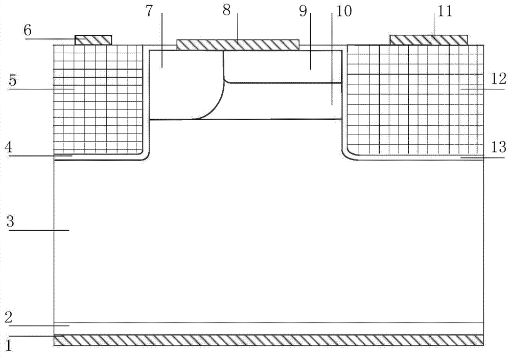
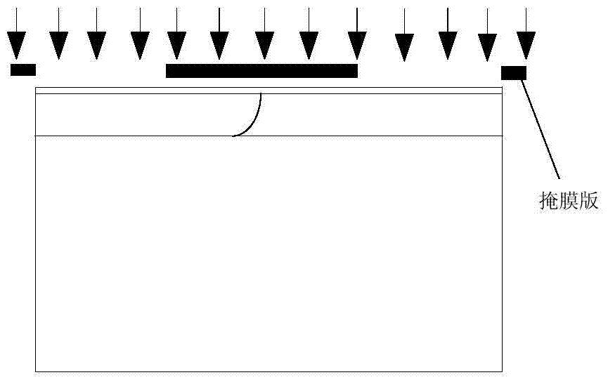
[0021] see figure 1 with 2 , the embodiment of the present invention is provided with a metallized collector electrode 1, a P-type collector region 2, an N-type drift region 3, a silicon dioxide side polysilicon oxide layer 4, a side polysilicon electrode 5, and a metallized side polysilicon electrode 6 , P+ body region 7 , metalized emitter 8 , N+ type source region 9 , P type base region 10 , metalized gate 11 , polysilicon gate electrode 12 and silicon dioxide gate oxide layer 13 .

[0022] The metallized collector 1 is located on the back of the P-type collector region 2, and the N-type drift region 3 is located on the front of the P-type collector region 2; the N+ type source region 9 and the P+ body region 7 are located side by side on the metallized emitter 8 Below, the N+ type source region 9 and the P+ body region 7 are connected to the met...


PUM


Abstract

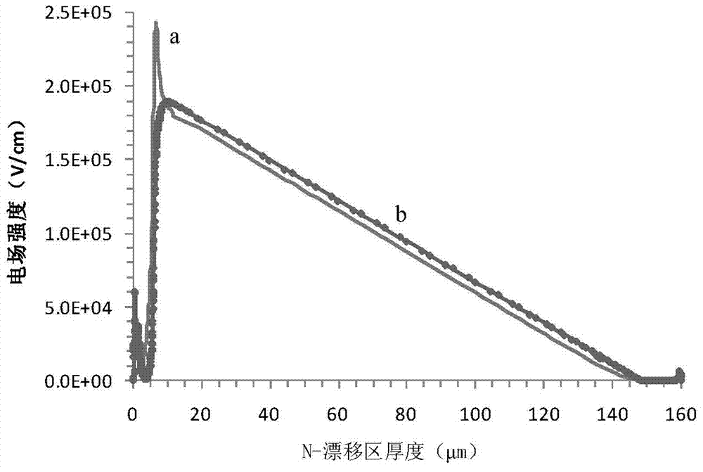
The invention discloses a non-punch-through type insulated gate bipolar transistor with a side polysilicon electrode trench, and relates to a bipolar transistor. The non-punch-through type insulated gate bipolar transistor is provided with a metalized collector electrode, a P type collector electrode region, an N- type drift region, a silicon dioxide side polysilicon oxide layer, a side polysilicon electrode, a metalized side polysilicon electrode, a P+ type body region, a metalized emitter electrode, an N+ type source region, a P type base region, a metalized gate electrode, a polysilicon gate electrode and a silicon dioxide gate oxide layer. A side polysilicon electrode technology is introduced in a traditional non-punch-through type insulated gate bipolar transistor with a trench; a mask plate does not need to be arranged and the junction depth of an original P+ type body region is expanded to be connected with the N- type drift region; a positive voltage is applied to Side-poly (the side polysilicon electrode trench), so that a reverse electric field can be generated, the shortcoming of electric field accumulation due to small bottom curve rate of the trench in Trench-NPT-IGBT (the non-punch-through type insulated gate bipolar transistor with the side polysilicon electrode trench) is overcome, and the peak electric field at the bottom of a trench gate is effectively reduced. Therefore, the non-punch-through type insulated gate bipolar transistor has the characteristics of higher breakdown voltage and lower threshold voltage.

Description

technical field [0001] The invention relates to a bipolar transistor, in particular to a non-penetrating insulated gate bipolar transistor with side polysilicon electrode trenches. Background technique [0002] Insulated gate bipolar transistor (IGBT) not only has the advantages of high input impedance of MOSFET, low driving power, low switching loss, but also high current density and low saturation voltage of bipolar power transistor. As a new type of power semiconductor device, it is widely used in the field of power electronics. However, since the IGBT is designed with trench gate technology, the electric field is easy to concentrate at the bottom of the trench gate due to the small surface ratio at the bottom of the trench, which limits the breakdown voltage of the trench gate type insulated gate field effect transistor. [0003] Literature [1] "Dual-Material-Gate Technique for Enhanced Transconductance and Breakdown Voltage of Trench Power MOSFETs" (Author: Raghvendra ...

Claims


Application Information

Patent Timeline
Patent Type & Authority Applications(China)
IPC IPC(8): H01L29/739H01L29/41
CPCH01L29/7397H01L29/423
Inventor 郭东辉江凌峰
Owner XIAMEN UNIV
Learn More