Light-emitting diode epitaxial growth method

A light-emitting diode and epitaxial growth technology, which is applied in the direction of electrical components, circuits, semiconductor devices, etc., can solve the problems of uneven wavelength distribution of epitaxial wafers, increased testing and sorting costs, and large wavelength dispersion of epitaxial wafers. And sorting cost, uniformity improvement, and the effect of improving warpage

Active Publication Date: 2014-02-05
EPITOP PHOTOELECTRIC TECH
View PDF4 Cites 10 Cited by
  • Summary
  • Abstract
  • Description
  • Claims
  • Application Information

AI Technical Summary

Problems solved by technology

[0003] For LEDs grown by traditional methods, due to the large warpage of the substrate, the wavelength distribution of the epitaxial wafer is uneven. The standard deviation of the wavelength (Standard Deviation, referred to as STD) is generally between 2-2.4nm, and the wavelength difference is generally Around 12nm, which reduces the quality of the LED
In addition, when LED chips are tested and sorted, because the wavelength dispersion of epitaxial wafers is large, it will increase the cost of testing and sorting

Method used


Image

  • Light-emitting diode epitaxial growth method
  • Light-emitting diode epitaxial growth method
  • Light-emitting diode epitaxial growth method

Examples


specific Embodiment 1

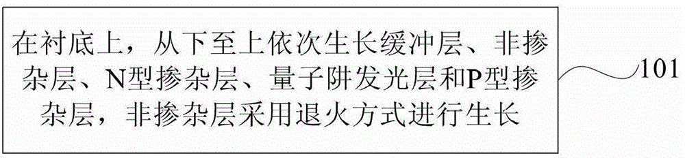
[0038] Specific embodiment one: 1 time annealing

[0039] figure 2 It is a schematic diagram of the temperature structure for one-time annealing epitaxial growth. Combine below figure 2 The light-emitting diode epitaxial growth method provided in this embodiment is described in detail, and the method includes:

[0040] 1. Put the sapphire (Patterned Sapphire Substrate, PSS for short) substrate into the reaction chamber, N 2 :H 2 : NH 3 The flow rate ratio is (0:120:0) liters per minute (Standard Liter per Minute, referred to as SLM), the reaction chamber pressure is 500 Torr Torr, the temperature is raised to 1080 ° C, stabilized for 300 seconds, and the substrate is purified at high temperature .

[0041] 2. Lower the temperature to 550°C, N 2 :H 2 : NH 3 The flow rate ratio is (75:150:56) SLM, the reaction chamber pressure is controlled at 500 Torr, and a low-temperature GaN buffer layer 21 with a thickness of 35 nm is grown.

[0042] 3. Raise the temperature to ...

specific Embodiment 2

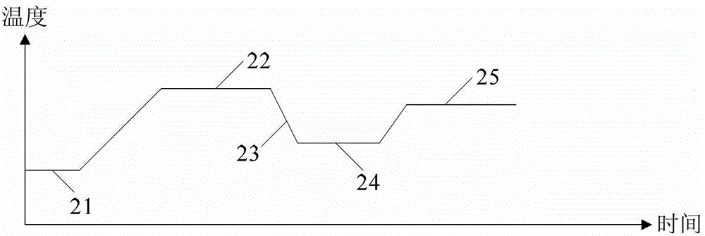
[0050] Specific embodiment two: 5 times of constant temperature annealing

[0051] image 3 It is a schematic diagram of the temperature structure for five times of isothermal annealing epitaxial growth. Combine below image 3 The light-emitting diode epitaxial growth method provided in this embodiment is described in detail, and the method includes:

[0052] 1. Put the sapphire PSS substrate into the reaction chamber, N 2 :H 2 : NH 3 The flow rate ratio is (0:120:0) SLM, the reaction chamber pressure is 500Torr, the temperature is raised to 1080°C, stabilized for 300 seconds, and the substrate is purified at high temperature.

[0053] 2. Lower the temperature to 550°C, N 2 :H 2 : NH 3 The flow rate ratio is (75:150:56) SLM, the reaction chamber pressure is controlled at 500 Torr, and a low-temperature GaN buffer layer 31 with a thickness of 35 nm is grown.

[0054] 3. Raise the temperature to 1080°C, N 2 :H 2 : NH 3 The flow rate ratio is (75:150:56) SLM, the reac...

specific Embodiment 3

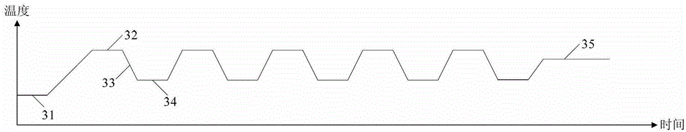
[0063] Specific embodiment three: 3 times of variable temperature annealing

[0064] Figure 4 It is a schematic diagram of the temperature structure for epitaxial growth with three temperature-variable annealings. Combine below image 3 The light-emitting diode epitaxial growth method provided in this embodiment is described in detail, and the method includes:

[0065] 1. Put the sapphire PSS substrate into the reaction chamber, N 2 :H 2 : NH 3 The flow rate ratio is (0:120:0) SLM, the reaction chamber pressure is 500Torr, the temperature is raised to 1080°C, stabilized for 300 seconds, and the substrate is purified at high temperature.

[0066] 2. Lower the temperature to 540°C, N 2 :H 2 : NH 3 The flow rate ratio is (75:150:56) SLM, the reaction chamber pressure is controlled at 500 Torr, and a low-temperature GaN buffer layer 41 with a thickness of 35 nm is grown.

[0067] 3. Raise the temperature to 1020°C, N 2 :H 2 : NH 3 The flow rate ratio is (75:150:56) SL...


PUM


Abstract

The invention provides a light-emitting diode epitaxial growth method. The method comprises the step of growing a buffer layer, undoped layers, an N-type doped layer, a quantum well light-emitting layer and a P-type doped layer on a substrate successively from bottom to up, wherein the undoped layers are grown through the annealing method. According to the light-emitting diode epitaxial growth method provided in the invention, the undoped layers are grown alternately through the annealing method, so the warping degree of the substrate in high-temperature conditions can be effectively improved, and the temperature uniformity of the bottom portion of the substrate can be improved, so that the wavelength distribution uniformity and the LED quality can be improved. Additionally, the test and sorting cost can be reduced to a certain extent.

Description

technical field [0001] The invention relates to the technical field of semiconductors, in particular to an epitaxial growth method of a light emitting diode. Background technique [0002] When Light Emitting Diode (LED) is grown by Metal-Organic Chemical Vapor Deposition (MOCVD), the uniformity of the wavelength of the epitaxial wafer has a great influence on the quality of the product. The better the wavelength uniformity of the epitaxial wafer and the smaller the wavelength distribution, the more beneficial it is for the production of LEDs with specific wavelengths. Since there is a certain lattice mismatch between the epitaxial layer (such as gallium nitride GaN epitaxial layer) and the substrate, the epitaxial layer will generate stress during MOCVD growth. If this part of the stress is not eliminated, the substrate will be A certain warpage occurs at high temperature, that is, a certain deformation of the substrate occurs. The distance between each part of the deforme...

Claims


Application Information

Patent Timeline
Patent Type & Authority Applications(China)
IPC IPC(8): H01L33/00
CPCH01L33/007H01L33/0075H01L33/06
Inventor 焦建军黄小辉李晓莹周德保郑远志陈向东康建梁旭东
Owner EPITOP PHOTOELECTRIC TECH
Why Eureka
Try Eureka