
Tantalum target and method for manufacturing tantalum target assembly

A manufacturing method and technology of tantalum target material, applied in the field of target material processing, can solve the problems of inability to meet the requirements of semiconductor sputtering process, uneven internal structure, coarse grains, etc.

Active Publication Date: 2016-05-04
KONFOONG MATERIALS INTERNATIONAL CO LTD
View PDF5 Cites 1 Cited by
  • Summary
  • Abstract
  • Description
  • Claims
  • Application Information

AI Technical Summary

Problems solved by technology

[0008] The problem to be solved by the present invention is that the existing tantalum target manufacturing method has uneven internal structure and coarse grains (grain size is 2 mm to 3 mm), which cannot meet the increasingly demanding semiconductor sputtering process.

Method used


Image

  • Tantalum target and method for manufacturing tantalum target assembly
  • Tantalum target and method for manufacturing tantalum target assembly
  • Tantalum target and method for manufacturing tantalum target assembly

Examples


Embodiment Construction

[0054] As described in the background art, in the prior art, the processing technology of plastically deforming high-purity tantalum ingots to produce high-purity tantalum targets for semiconductors involves less and is not perfect. Therefore, how to produce The tantalum target material has become one of the most important problems to be solved at present.

[0055] PVD is usually carried out by magnetron sputtering. The so-called magnetron sputtering means that the plasma generated by the rare gas bombards the surface of the cathode sputtering target under the interaction of the electric field and the magnetic field, so that the molecules on the surface of the target, Atoms and electrons are sputtered out, and the sputtered particles have a certain kinetic energy, and shoot to the surface of the substrate in a certain direction, and deposit on the surface of the substrate to form a coating. The inventors found that during the coating process by magnetron sputtering, the positi...


PUM

PropertyMeasurementUnit
sizeaaaaaaaaaa
particle sizeaaaaaaaaaa
sizeaaaaaaaaaa

Abstract

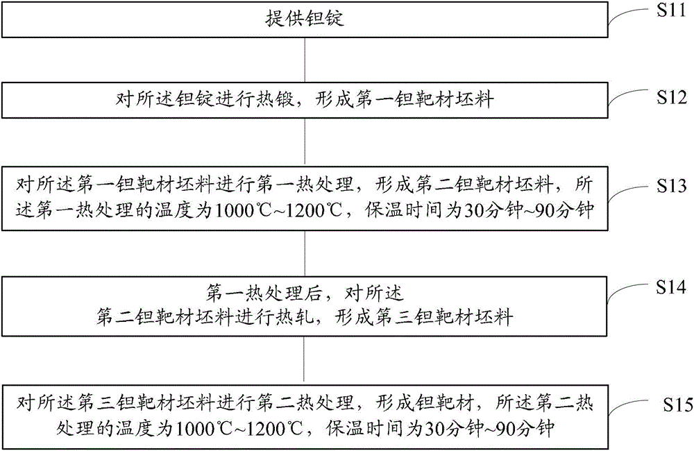
The invention provides a production method of a tantalum target and a tantalum target component. The production method of a tantalum target comprises the following steps of providing a tantalum ingot; performing hot forging on the tantalum ingot to form a first tantalum target blank; performing first heat treatment on the first tantalum target blank to form a second tantalum target blank, wherein the temperature of the first heat treatment is 1,000-1,200 DEG C, and the temperature is maintained for 30-90 minutes; after the first heat treatment, performing hot rolling on the second tantalum target material to form a third tantalum target blank; performing second heat treatment on the third tantalum target blank to form the tantalum target, wherein the temperature of the second heat treatment is 1,000-1,200 DEG C, and the temperature is maintained for 30-90 minutes. By adopting the technical scheme, the produced tantalum target has relatively uniform internal organization and good magnetic property; moreover, by adopting the tantalum target to produce a tantalum target component for a semiconductor, the formed film has relatively good quality.

Description

technical field [0001] The invention relates to the field of target processing, in particular to a method for manufacturing a tantalum target and a tantalum target assembly. Background technique [0002] Physical Vapor Deposition (PVD, Physical Vapor Deposition) is widely used in high-end industries such as optics, electronics, and information, such as: integrated circuits, liquid crystal displays (LCD, Liquid Crystal Display), industrial glass, camera lenses, information storage, ships, chemicals, etc. Metal target components used in PVD are one of the most important raw materials in the manufacturing process of integrated circuits and liquid crystal displays. [0003] The metal target component is composed of a metal target that meets the sputtering performance and a back plate with a certain strength. The back plate can play a supporting role when the metal target assembly is assembled to the sputtering base station, and has the effect of conducting heat. With the conti...

Claims


Application Information

Patent Timeline
Patent Type & Authority Patents(China)
IPC IPC(8): C23C14/34C22F1/18
Inventor 姚力军相原俊夫大岩一彦潘杰王学泽陈勇军
Owner KONFOONG MATERIALS INTERNATIONAL CO LTD
Learn More