V-shaped coupled cavity tunable semiconductor laser unit capable of directly conducting modulation at high speed

A coupled cavity and semiconductor technology, applied in the field of high-speed direct-tuning V-shaped coupled cavity tunable semiconductor lasers, can solve the problems of large difference in power between different channels, high laser noise level, influence of laser life, etc., and achieves simple structure and high yield. , the effect of increasing the stability of the module

Inactive Publication Date: 2014-02-12
ZHEJIANG UNIV
View PDF2 Cites 9 Cited by
  • Summary
  • Abstract
  • Description
  • Claims
  • Application Information

AI Technical Summary

Problems solved by technology

This kind of laser can realize digital switching of more than 20 channels with an interval of 100 GHz, but because this design only sets a passive tuning area in one of the two FP resonators that constitute the V cavity, the rest of the laser They are all active, although more than 20 channels can be switched, and the lasing current threshold is relatively low, but the speed of high-speed direct modulation is limited by the wavelength mode hopping caused by the change of carrier concentration in the cavity, because the injection in the laser coupler After the microwave signal, the carrier levels of the two FP resonators vary inconsistently, and lasing mode hopping is prone to occur, which greatly limits the application of this design; and this design wants to expand the tuning range to cover the entire C-band or For a larger range, it will be necessary to continuously increase the current in the active region to generate heat to move the gain spectrum. Due to the injection of large current, the noise level of the laser will be high, the linewidth characteristics will deteriorate, and the power between different channels The difference is also very large, and it will also have a significant impact on the life of the laser

Method used


Image

  • V-shaped coupled cavity tunable semiconductor laser unit capable of directly conducting modulation at high speed
  • V-shaped coupled cavity tunable semiconductor laser unit capable of directly conducting modulation at high speed
  • V-shaped coupled cavity tunable semiconductor laser unit capable of directly conducting modulation at high speed

Examples


Embodiment Construction

[0030] The present invention will be further described below in conjunction with the accompanying drawings and embodiments.

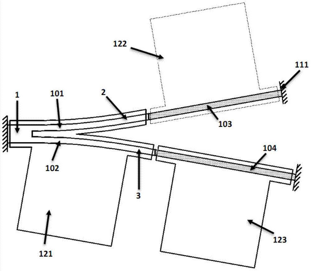
[0031] Such as figure 2 Shown is the first embodiment of the high-speed direct V-coupled cavity tunable semiconductor laser of the present invention. The present invention includes a half-wave coupler 1, a wavelength reference FP resonant cavity and a wavelength tuning FP resonant cavity; the wavelength reference FP resonant cavity 2 is composed of a short-cavity active waveguide 101 and a short-cavity passive waveguide 103 connected in series, and the wavelength tuning FP Resonant cavity 3 is composed of long-cavity active waveguide 102 and long-cavity passive waveguide 104; The optical length ratio of the waveguide 104; the short-cavity active waveguide 101 and the long-cavity active waveguide 102 are provided with a modulation signal electrode 121, and the long-cavity passive waveguide 104 is provided with a wavelength tuning electrode 123.

[003...


PUM


Abstract

The invention discloses a V-shaped coupled cavity tunable semiconductor laser unit capable of directly conducting modulation at a high speed. The V-shaped coupled cavity tunable semiconductor laser unit comprises a semi-wave coupler, a wave length reference FP resonant cavity and a wave length tuning FP resonant cavity, wherein short cavity active waveguide and short cavity passive waveguide are connected in series to form the wave length reference FP resonant cavity, long cavity active waveguide and long cavity passive waveguide are connected in series to form the wave length tuning FP resonant cavity, the ratio of the optical length of the short cavity active waveguide to the optical length of the short cavity passive waveguide is equal to the ratio of the optical length of the long cavity active waveguide to the optical length of the long cavity passive waveguide, and therefore the mode jump does not occur when the laser unit directly conducts modulation at the high speed. The laser unit can further comprise a section of thin film resistor added to the top of the semi-wave coupler so that the tuning range can be enlarged, and comprise two sections of active waveguide added outside cavities and deep etching grooves so that the threshold of the laser unit can be reduced, and an optical power meter integrated on a piece is provided. According to the V-shaped coupled cavity tunable semiconductor laser unit, the C wave section and sections in a wider range can be tuned, and performance of conducting direct modulation on each communication wave with the wave length more than 10Gbps is achieved.

Description

technical field [0001] The invention relates to a semiconductor laser, in particular to a high-speed direct modulation V-type coupled cavity tunable semiconductor laser. Background technique [0002] High-speed direct modulation broadband tunable semiconductor lasers are widely used in access networks and data exchange networks. Not only can it be used as a backup light source to reduce inventory costs, but it can also be used to design more intelligent optical networks or optical modules. For example, a tunable laser and a wavelength division multiplexing device can realize a reconfigurable optical upload and download multiplexer; a tunable laser can also form a wavelength converter together with a semiconductor optical amplifier. [0003] Most of the currently proposed single-chip integrated wide-range tunable semiconductor lasers are based on grating mode selection. These lasers need to make gratings, the process is very complicated, and the required epitaxial wafer area...

Claims


Application Information

Patent Timeline
Patent Type & Authority Applications(China)
IPC IPC(8): H01S5/14H01S5/024H01S5/026
Inventor 武林邓浩瑜孟剑俊何建军
Owner ZHEJIANG UNIV
Why Eureka
Try Eureka