Laser diode with p type substrate
A laser diode, p-type technology, used in lasers, laser parts, semiconductor lasers, etc., can solve the problems of shortened laser diode life, reduced quality and performance of epitaxial layers on substrates, crystal strain, etc., to reduce defect density, The effect of improving the recombination probability and improving the luminous efficiency
- Summary
- Abstract
- Description
- Claims
- Application Information
AI Technical Summary
Problems solved by technology
Method used
Image

Examples
Embodiment Construction
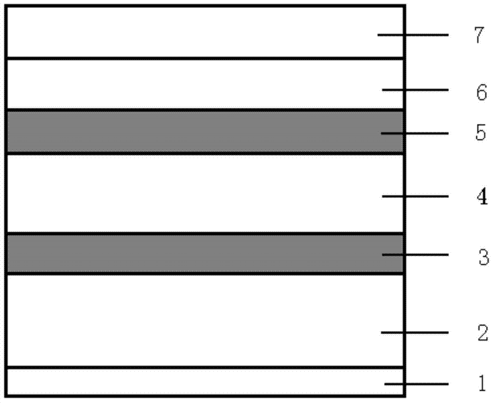
[0015] see figure 1 , the laser diode of the present invention includes a p-GaN substrate 2, wherein, a p-electrode 1 is arranged under the p-GaN substrate 2; a p-type interface layer 3, a light-emitting layer 4, and an n-type interface layer 3 are sequentially arranged on the p-GaN substrate 2 Interface layer 5, n-type injection layer 6, n-electrode 7;
[0016] Wherein, the p-type interface layer 3 is p-Al x In y Ga 1-x-y P, wherein 0
[0017] Wherein, the light-emitting layer 4 is a multi-quantum well layer of superlattice structure, and the material of the multi-quantum well layer is ZnO / Zn 1-a Mg a O / Zn 1-b As b O, where 01-a Mg a O / Zn 1-b As b O composition. The structure of the light-emitting layer is specifically: the ZnO layer has Zn 1-a Mg a O layer and Zn 1-b As b O layer, these three layers form a sandwich structure, and every three layers are regarded as a cycle, in the present invention, ...
PUM
 Abstract
Description
Claims
Application Information
 - Generate Ideas
- Intellectual Property
- Life Sciences
- Materials
- Tech Scout
- Unparalleled Data Quality
- Higher Quality Content
- 60% Fewer Hallucinations
Browse by: Latest US Patents, China's latest patents, Technical Efficacy Thesaurus, Application Domain, Technology Topic, Popular Technical Reports.
© 2025 PatSnap. All rights reserved.Legal|Privacy policy|Modern Slavery Act Transparency Statement|Sitemap|About US| Contact US: help@patsnap.com