A shifting register unit, a grid electrode driving circuit, and a display

A shift register and driving voltage technology, applied in static memory, static indicators, digital memory information, etc., can solve the problems of large layout area, increase of peripheral circuit load and total power consumption, occupation, etc., and achieve a small layout occupation area , reduced rise and fall times, and reduced complexity

Active Publication Date: 2014-03-05
PEKING UNIV SHENZHEN GRADUATE SCHOOL
View PDF5 Cites 24 Cited by
  • Summary
  • Abstract
  • Description
  • Claims
  • Application Information

AI Technical Summary

Problems solved by technology

This will not only occupy a larger layout area, but also increase the load on the peripheral lines and the total power consumption

Method used


Image

  • A shifting register unit, a grid electrode driving circuit, and a display
  • A shifting register unit, a grid electrode driving circuit, and a display
  • A shifting register unit, a grid electrode driving circuit, and a display

Examples


Embodiment 1

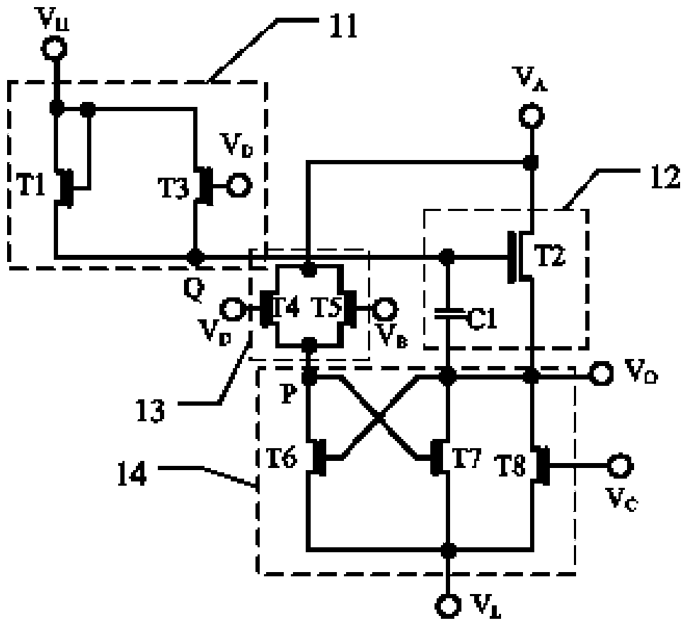
[0056] The shift register unit is a very important unit circuit to realize the gate drive circuit, such as figure 1 with figure 2 As shown, the shift register unit of this embodiment includes a charging and discharging module 11 , a driving module 12 , a low-level maintaining enabling module 13 and a low-level maintaining module 14 .

[0057] The signal input terminals of the charging and discharging module 11 are respectively connected to the pulse signal input terminal and the fourth clock signal input terminal for inputting the pulse signal V I1 and the fourth clock signal V D ; The clock input end of the drive module 12 is connected to the first clock signal input end, and the first clock signal V is input A , the drive module 12 has a drive enabling control terminal Q, the output terminal of the charging and discharging module 11 is connected to the driving enabling control terminal Q of the driving module 12, and the charging and discharging module 11 is used to input...

Embodiment 2

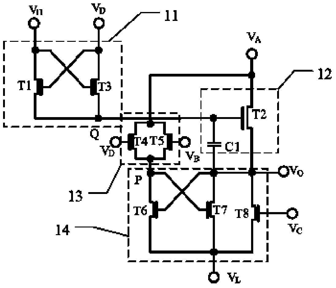
[0095] As shown in Fig. 4, it is the circuit diagram of the embodiment of the second shift register unit, the shift register unit of this embodiment includes a pair of subunit circuits, wherein one subunit circuit is as Figure 4-a As shown, it includes: drive module A12, charge and discharge module A11, low level maintenance module A14 and low level maintenance enabling module A13; another subunit circuit such as Figure 4-b As shown, it includes: a driving module B12, a charging and discharging module B11, a low level maintaining module B14 and a low level maintaining enabling module B13. The only difference between the two is that the signal input of the low-level maintenance enabling module A13 includes the first extended clock signal ECK1, while the signal input of the corresponding port of the low-level maintenance enabling module B13 is the same as the first extended clock signal ECK1. Complementary second extended clock signal ECK2.

[0096] The signal input terminals...

Embodiment 3

[0109] Such as Figure 5 Shown is a structural block diagram of a gate drive circuit disclosed in the present invention. The gate drive circuit includes a shift register, and the shift register uses N+1 stages of shift register units in series as described in the above-mentioned embodiment 1. Where N is a positive integer. The gate drive circuit also includes a first clock line line1, a second clock line line2, a third clock line line3, a fourth clock line line4, and a general common ground line L-V L and a start signal line STV. Wherein, the signal output terminals of the driving circuit units of the first level to the Nth level provide the gate driving signal V for the pixel array. G 1 ~V G N , and V G 1 ~V G N They are respectively coupled to the pulse signal input terminals of their own next-stage shift register units, and are used to start the next-stage shift register units; the N+1th stage is an additional stage, V G N+1 Return the pulse signal input end of t...


PUM


Abstract

The application discloses a shifting register unit, a grid electrode driving circuit, and a display. The shifting register unit comprises a first clock signal input end, a four clock signal input end, a pulse signal input end, a signal output end, a driving module, a charging and discharging module, a low level maintaining module, and a low level maintenance enablement module. By means of the superposition of multiphase clock signals, the shifting register unit decreases the positive voltage bias duty ratio of a TFT of the low level maintenance enablement module, and introduces the negative voltage bias time of the TFT of the low level maintenance enablement module. Therefore, the threshold voltage drift of the low level maintenance enablement module is decreased and the stability of a pull-down circuit is enhanced. The grid electrode driving circuit formed by the shifting register unit and a pixel TFT are produced on a display panel together. Therefore, the number of the external pins and the peripheral chips of the display panel is decreased and integration degree of the display panel is enhanced.

Description

technical field [0001] The present application relates to a display, in particular to a gate drive circuit and a shift register unit of the display. Background technique [0002] Flat panel display technology (FPD) based on thin film transistors (TFT) is the mainstream of display technology today. For a long time, System on Panel (SOP) has been a goal pursued by the flat panel display field. In the SOP panel, the peripheral driver circuit of the display and the TFT driver array are integrated on the same substrate. Compared with the panel using the conventional external drive circuit, the SOP display panel has the following advantages: (1) the number of row and column drive chips is small; (2) the number of row and column drive chips and the display panel is small; (3 ) The frame of the display panel is narrower, and the display module will be more compact and beautiful; (4) It can reduce the limitation of the pitch between the leads to the realization of high-resolution d...

Claims


Application Information

Patent Timeline
Patent Type & Authority Applications(China)
IPC IPC(8): G09G3/20G11C19/28
Inventor 张盛东廖聪维胡治晋
Owner PEKING UNIV SHENZHEN GRADUATE SCHOOL
Why Eureka
Try Eureka