Polymer-based optically variable devices
A polymer and device technology, used in optical components, instruments, thin material processing, etc., can solve problems such as random changes in color
- Summary
- Abstract
- Description
- Claims
- Application Information
AI Technical Summary
Problems solved by technology
Method used
Image

Examples
Embodiment 1
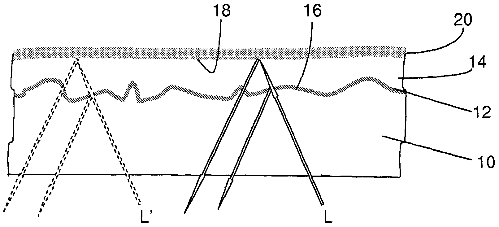
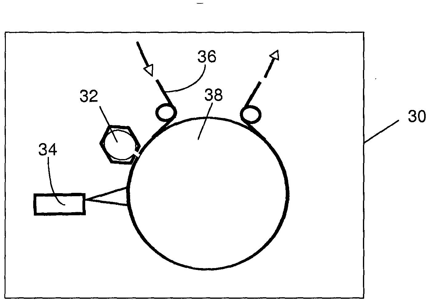
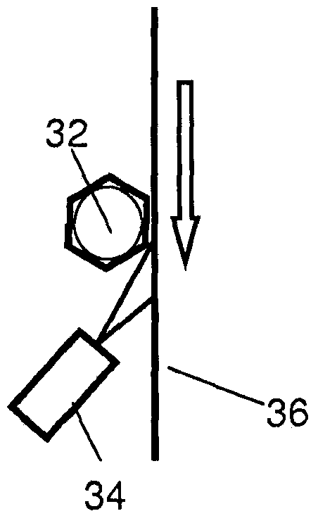
[0042] Example 1. This example demonstrates that substrates with significant levels of microroughness, when leveled with a leveling layer, can produce OVDs without significant color change. Optically variable devices were formed on a 1-mil (ie, 1 / 1000th of an inch) thick, 60-inch wide PET film substrate with a haze of 5% or greater and a gloss of 90% or less. PET film was first coated at a speed of 2.5 m / s with a 0.6 micron thick layer of leveling polymer obtained by depositing propoxylated (2) neopentyl glycol diacrylate on the PE film The monomer is then cured with an electron beam curtain to form. A layer of aluminum was then deposited across the PET mesh on a leveling layer with a uniform optical density of 0.35 and a uniform emissivity of 0.5. A thin layer of aluminum is then coated with a spacer liner composed of the same polymer as the leveling layer at a web speed of 0.6 m / s to 1.2 m / s. The spacer liner is then coated with a relatively opaque layer of aluminum. Exa...
Embodiment 2
[0043] Example 2. The conditions of Example 2 were repeated, except that a layer of chromium was coated with a uniform optical density of 0.4 across the width of the film, and an emissivity of 0.65 with a variation of less than + / - 0.06 across a width of 30" 30" wide, 2-mil thick PET film with less than 1% haze and >95% gloss. At constant velocity, PET maintained at room temperature and moving at a speed of 0.6m / s-1.2m / s A monomer formulation consisting of 5% beta carboxyethyl acrylate, 45% Zonyl TM / TA-N, 5% hexanediol diacrylate and 45% tripropylene glycol diacrylate was flashed on the web. An electron beam curtain close to the monomer deposition station polymerizes the monomer layer so that the time between deposition and curing is less than 2 seconds. By depositing a polymer layer followed by an opaque aluminum layer, a series of OVD devices were produced and showed The following color shifts:
[0044] dark blue with little or no transfer;
[0045] Light green transfers ...
Embodiment 3
[0054] Example 3. Optically variable devices were formed on a 12 micron thick PET substrate with less than 1% haze and greater than 95% gloss. A stainless steel layer was deposited on a PET substrate with an average emissivity of 0.66 and an optical density OD=0.5. Across the deposition area, the emissivity varies by less than 0.05. Using, a monomer formulation consisting of 95 parts propoxylated neopentyl glycol diacrylate and 5 parts acidic acrylate oligomer was designed to reduce the heat sensitivity of the monomer and provide metal adhesion. The monomer was condensed on the SS substrate at a web velocity of 5 m / s. The condensed monomer layer was e-beam cured within 2 seconds of deposition and a relatively opaque aluminum layer. Using an optical interferometer with two sensing heads across the polymer mesh, the color is measured and the layer thickness of the polymer is controlled. The thickness of the deposited polymer layer was varied, forming a color shift pattern, a...
PUM
 Abstract
Description
Claims
Application Information
 - R&D
- Intellectual Property
- Life Sciences
- Materials
- Tech Scout
- Unparalleled Data Quality
- Higher Quality Content
- 60% Fewer Hallucinations
Browse by: Latest US Patents, China's latest patents, Technical Efficacy Thesaurus, Application Domain, Technology Topic, Popular Technical Reports.
© 2025 PatSnap. All rights reserved.Legal|Privacy policy|Modern Slavery Act Transparency Statement|Sitemap|About US| Contact US: help@patsnap.com