
Physical vapor deposition device and method for Nano silicon-crystal thin film of solar battery

A technology of physical vapor deposition and solar cells, applied in the direction of ion implantation plating, metal material coating process, coating, etc., can solve the limitation of photoelectric conversion efficiency and the improvement of service life, and solar cells cannot fundamentally solve the problem of light decay and migration , Diffusion ability is very poor and other problems, to achieve the effects of photoelectric conversion efficiency, large beam current, and wide energy regulation range

Inactive Publication Date: 2006-04-19
吴大维
View PDF0 Cites 11 Cited by
  • Summary
  • Abstract
  • Description
  • Claims
  • Application Information

AI Technical Summary

Problems solved by technology

[0007] In contrast to silane SiH 4 Glow discharge PCVD deposits microcrystalline silicon thin films. Due to the lower excited energy state of silane, compared with amorphous silicon, although the grain size has increased, it still contains a higher ratio of hydrogen atoms. This silicon thin film is used to make solar energy Batteries cannot fundamentally solve the problem of light decay
Microcrystalline silicon is deposited by glow discharge. The excited silicon atomic group has a low energy state in the electric field. Its motion state is a drift behavior. It has poor migration and diffusion capabilities during the deposition process, and it is impossible to avoid the formation of a large number of lattices in the film. Defects, this kind of high-defect random network, must use hydrogen atoms to saturate the dangling bonds, and it is inseparable from hydrogen atoms, so this method of making solar cells with silicon thin films greatly limits the improvement of photoelectric conversion efficiency and service life

Method used


Image

  • Physical vapor deposition device and method for Nano silicon-crystal thin film of solar battery
  • Physical vapor deposition device and method for Nano silicon-crystal thin film of solar battery
  • Physical vapor deposition device and method for Nano silicon-crystal thin film of solar battery

Examples


Embodiment Construction

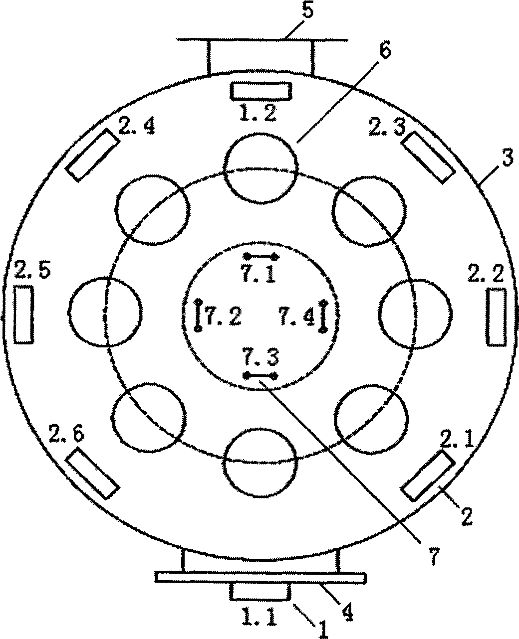
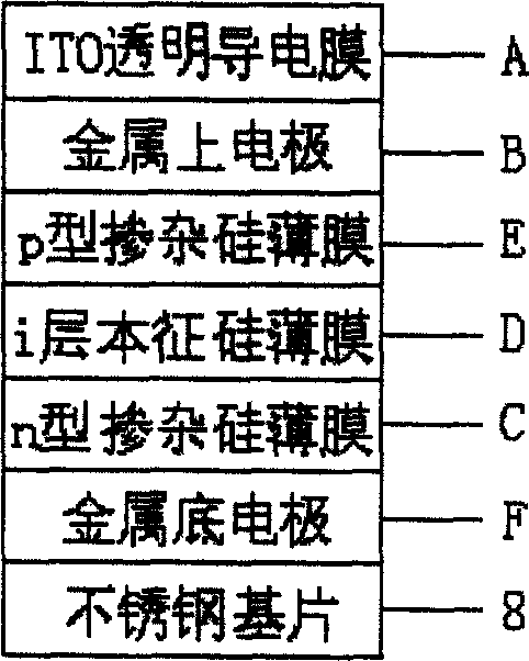
[0055] Example: Take the stainless steel substrate 8 as an example to illustrate the specific implementation process.

[0056] 1. Substrate polishing and cleaning

[0057] The stainless steel substrate 8 is mechanically polished, the surface is smooth and bright without scratches, and the reflection coefficient is >85%. Then it is chemically cleaned, dehydrated and dried for later use.

[0058] 2. Racking

[0059] The cleaned stainless steel substrate 8 is loaded on the workpiece frame 6 and hung on the working rotating shaft in the vacuum chamber 3 . Maintain the cleanliness of the substrate and vacuum chamber components throughout the operation.

[0060] 3. Vacuuming

[0061] Close the furnace door 4, and pump a high vacuum to 3×10 according to the operation regulations of the coating machine. -3 Pa.

[0062] 4. Substrate baking

[0063] Vacuum up to 3×10 -3 After Pa, turn on the baking heating power supply to bake the substrate, control the baking temperature at 280...


PUM


Abstract

A physical evaporation deposition apparatus for preparing the nano-crystal silicon film of solar cell is based on the vacuum evaporation coating machine but has the physical evaporation deposit function. It method includes such steps as designing the figuration of vacuum evaporation coating machine, using ion beam method to deposit nano-crystal silicon film, and gas-phase doping to prepare the PIN structure of solar cell. Its advantage is high photoelectric conversion efficiency.

Description

technical field [0001] The invention relates to a method for making a solar cell nanocrystalline silicon thin film in the field of new energy materials; in particular, it relates to a physical vapor deposition (PVD) method for depositing a solar cell nanocrystalline silicon thin film by a plasma ion beam. Background technique [0002] Amorphous silicon (a-Si:H) thin-film solar cells have made great progress in basic theoretical research and production technology in recent years, and the photoelectric conversion efficiency has been continuously improved, which has become an important aspect of the promotion and application of solar cells on the ground. ([1] Edited by Chen Guanghua and Deng Jinxiang, New Electronic Thin Film Materials, Chemical Industry Press). The material structure of amorphous silicon is different from that of a perfect single crystal. Its microstructure is a random network of covalent bonds, short-range order, long-range disorder, and no lattice periodicit...

Claims


Application Information

Patent Timeline
IPC IPC(8): C23C14/24C23C14/56
Inventor 吴大维吴越侠徐建平
Owner 吴大维
Learn More