Self-powered photodetector based on Cs3Cu2I5 perovskite and preparation method thereof

A photodetector and self-powered technology, which is applied in circuits, electrical components, semiconductor devices, etc., can solve problems such as environmental pollution and structural stability, and achieve important scientific significance and practical value, environmental friendliness, and structural stability.

Active Publication Date: 2019-11-15
ZHENGZHOU UNIV
View PDF7 Cites 11 Cited by
  • Summary
  • Abstract
  • Description
  • Claims
  • Application Information

AI Technical Summary

Problems solved by technology

[0005] The purpose of the present invention is to propose a Cs-based 3 Cu 2 I 5 The self-powered photodetector of perovskite and its preparation method can realize the efficient detection of ultraviolet light, and overcome the environmental pollution problem faced by traditional lead halide perovskite

Method used


Image

  • Self-powered photodetector based on Cs3Cu2I5 perovskite and preparation method thereof
  • Self-powered photodetector based on Cs3Cu2I5 perovskite and preparation method thereof
  • Self-powered photodetector based on Cs3Cu2I5 perovskite and preparation method thereof

Examples


preparation example Construction

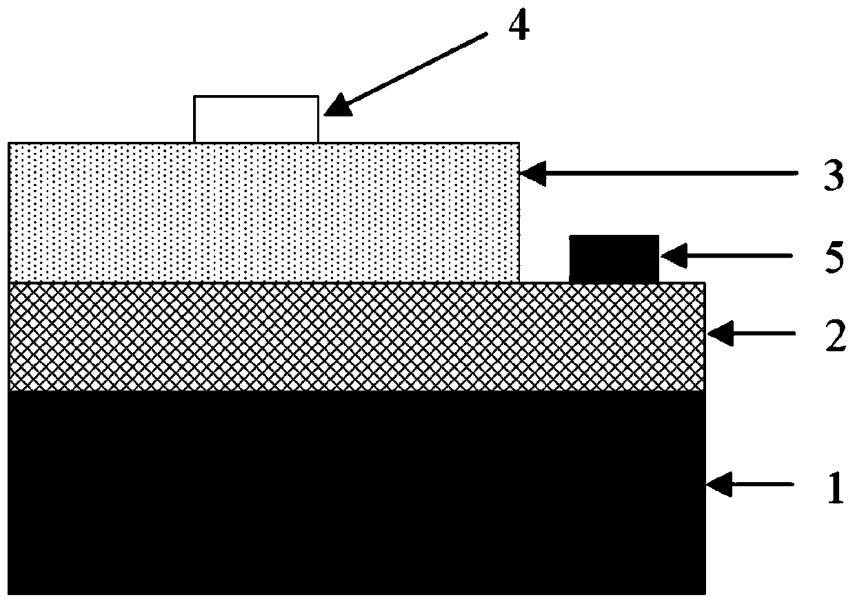
[0049] One of the above-mentioned Cs-based 3 Cu 2 I 5 The preparation method of the self-powered photodetector of perovskite comprises the following steps:

[0050] (1) cleaning the substrate 1;

[0051] (2) preparing the carrier transport layer 2 by magnetron sputtering or metal-organic chemical vapor deposition;

[0052] (3) Prepare Cs on the carrier transport layer 2 by one-step spin coating method or vapor phase co-evaporation method 3 Cu 2 I 5 light absorbing layer 3;

[0053] (4) using thermal evaporation method in Cs 3 Cu 2 I 5 A first contact electrode is prepared on the light absorbing layer 3 , and a second contact electrode 5 is prepared on the carrier transport layer 2 .

[0054] In the step (3), Cs 3 Cu 2 I 5 The light-absorbing layer 3 is prepared by a one-step spin-coating method, and toluene is added dropwise as an anti-solvent during the spin-coating process to ensure that the perovskite crystallizes rapidly and has a large surface coverage.

[0...

Embodiment 1

[0058] (1) Cleaning the substrate 1, which is a quartz substrate.

[0059] Use quartz as the substrate, and clean it. The cleaning steps are: put the substrate in acetone, ethanol, and deionized water for 10 minutes, and then recirculate once; then dry it with high-purity nitrogen; then, put the substrate Treat with a plasma cleaner, the gas used is argon, and the treatment time is 10 minutes.

[0060] (2) Prepare an n-type ZnO thin film as the carrier transport layer 2 .

[0061] Put the cleaned quartz substrate into the magnetron sputtering chamber, and use RF power to complete the sputtering of the ZnO carrier transport layer. The specific steps are: install the ZnO target, and adjust the position between the target and the substrate to 8 cm; turn on the mechanical pump to evacuate the sputtering chamber, when the vacuum of the chamber is lower than 10 Pascals, turn on the molecular pump and continue to evacuate until the vacuum of the chamber is lower than 5.0×10 -4 Pasc...

Embodiment 2

[0071] (1) Transparent quartz is used as the substrate. The cleaning method for the quartz substrate in this embodiment is the same as that in Embodiment 1.

[0072] (2) The n-type ZnO thin film was prepared as the carrier transport layer on the quartz substrate by magnetron sputtering method. The sputtering method for the n-type ZnO thin film in this embodiment is the same as that in Embodiment 1.

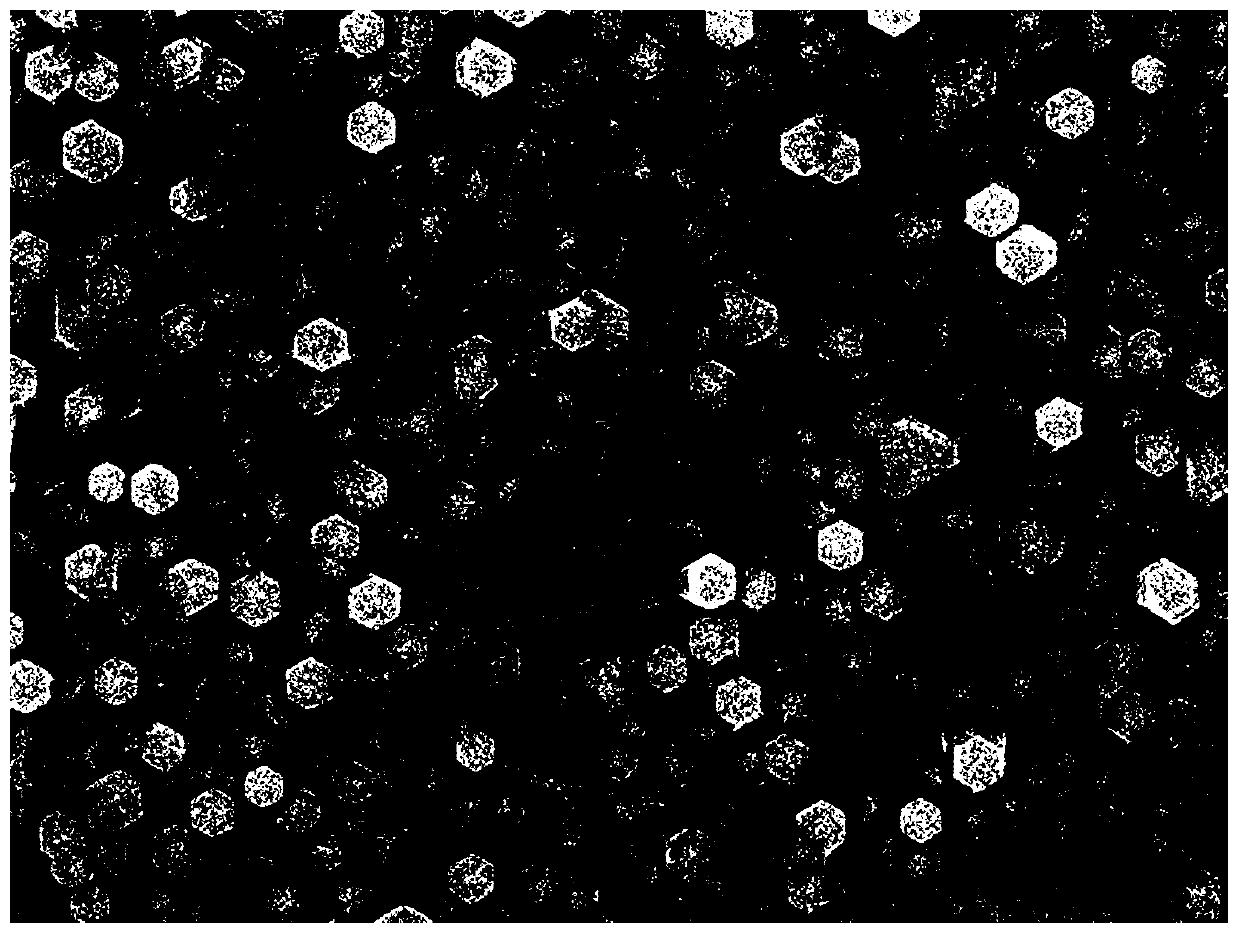
[0073] (3) Prepare Cs by vapor phase co-evaporation on the prepared ZnO carrier transport layer 2 3 Cu 2 I 5 Light absorbing layer 3.

[0074] 1) First, weigh 0.234 grams of CsI and 0.114 grams of CuI with a high-precision electronic balance; then, grind the CsI and CuI powders evenly and put them into a vacuum evaporation chamber;

[0075] 2) Place the substrate prepared with the carrier transport layer on the mixed powder of CsI and CuI; heat-treat the substrate at a temperature of 100°C, and evaporate at this temperature; wait until the pressure of the chamber drops to 10 ...


PUM


Abstract

The invention belongs to the technical field of semiconductor photodetection, and particularly relates to a self-powered photodetector based on Cs3Cu2I5 perovskite and a preparation method thereof. The self-powered photodetector includes an insulating transparent substrate, the upper end of the substrate is provided with a carrier transport layer, a Cs3Cu2I5 light absorption layer and a first contact electrode sequentially from bottom to top, and a second contact electrode is arranged on the carrier transport layer. According to the preparation method, the carrier transport layer is prepared by adopting a magnetron sputtering or metal organic chemical vapor deposition method, the Cs3Cu2I5 light absorption layer is prepared by adopting a solution or vapor phase co-evaporation method, staggered energy band arrangement is ensured to be formed between the carrier transport layer and the Cs3Cu2I5 light absorption layer, the formation of a built-in electric field at the interface of a heterojunction is used to enable photogenerated carriers to be separated, and the detector can thus work under zero volt. The preparation method is simple, each functional layer is environment-friendly, theprepared device has a high detection rate for ultraviolet light, the ultraviolet-visible light suppression ratio exceeds 10 of the fourth power, and the application prospect is good.

Description

technical field [0001] The invention belongs to the technical field of semiconductor photodetection, in particular to a Cs-based 3 Cu 2 I 5 Perovskite self-powered photodetectors and methods for their fabrication. Background technique [0002] In recent years, metal halide perovskite materials have attracted widespread attention due to their superior optical and electrical properties, and have shown great potential in the fields of solar cells, light-emitting diodes, photodetectors, and lasers. At present, there are many reports on photodetectors based on perovskite materials, such as photoconductive detectors, photovoltaic detectors, avalanche detectors, etc. Comparable to traditional inorganic semiconductors and two-dimensional materials, it has become a hot direction for the application of perovskite materials. [0003] However, based on traditional lead halide perovskites (CH 3 NH 3 wxya 3 , CsPbX 3 , X=Cl / Br / I) optoelectronic devices have been unsatisfactory in ...

Claims


Application Information

Patent Timeline
Patent Type & Authority Applications(China)
IPC IPC(8): H01L31/102H01L31/032H01L31/0224H01L31/18
CPCH01L31/022408H01L31/032H01L31/102H01L31/18Y02P70/50
Inventor 史志锋李营马壮壮梁文晴李新建
Owner ZHENGZHOU UNIV
Why Eureka
Try Eureka