Micro/nano array and application thereof in micro/nano material standard bending strain loading

A technology of nano-materials and bending strain, applied in metal material coating technology, micro-structure technology, micro-structure devices, etc., to achieve the effect of simple and clear strain state, simple operation mode and simple operation

Active Publication Date: 2014-03-26
PEKING UNIV
View PDF8 Cites 10 Cited by
  • Summary
  • Abstract
  • Description
  • Claims
  • Application Information

AI Technical Summary

Problems solved by technology

However, none of the above methods for aligning one-dimensional micro/nanomaterials for bending strain load

Method used


Image

  • Micro/nano array and application thereof in micro/nano material standard bending strain loading
  • Micro/nano array and application thereof in micro/nano material standard bending strain loading
  • Micro/nano array and application thereof in micro/nano material standard bending strain loading

Examples


Embodiment 1

[0044] Embodiment 1, preparation micro / nano support array

[0045] 1) Spin-coat SU-8 photoresist on the substrate at a speed of 500rpm for 10 seconds, then spin-coat at a speed of 3000rpm for 60 seconds, then keep at 65°C for 1 minute and then increase the temperature at 2°C / s The temperature was raised to 95° C. for 3 minutes for pre-baking to obtain a photoresist layer with a thickness of 15 μm.

[0046] 2) Use a photolithographic mask with a pre-designed pattern to mask, and use ultraviolet light to expose the photoresist layer (such as SU-8 photoresist) obtained in step 1) at an exposure dose of 13mW / cm 2 1. Expose under the condition that the exposure time is 12s, and then develop with SU-8 photoresist special developer (PGMEA—MicroChem, USA) for 4 minutes, remove the unexposed SU-8 photoresist, and get Micro / nano support arrays.

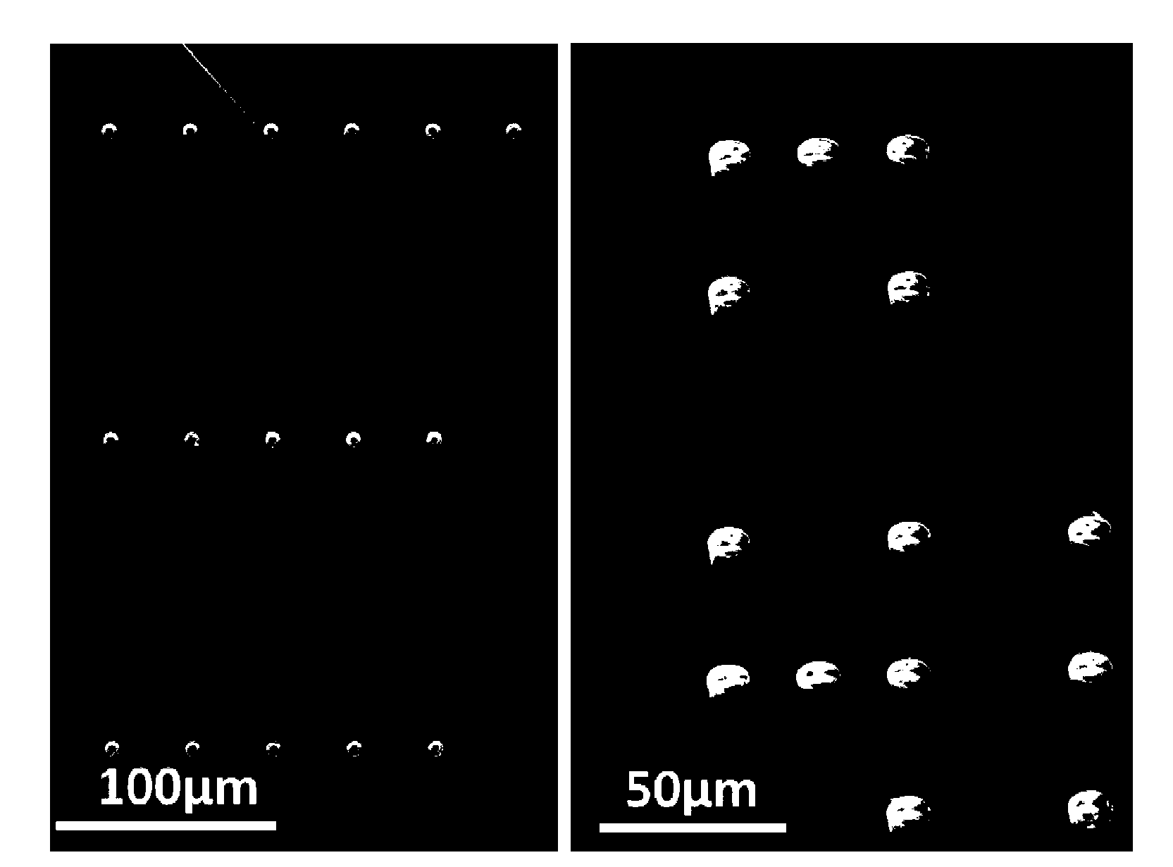
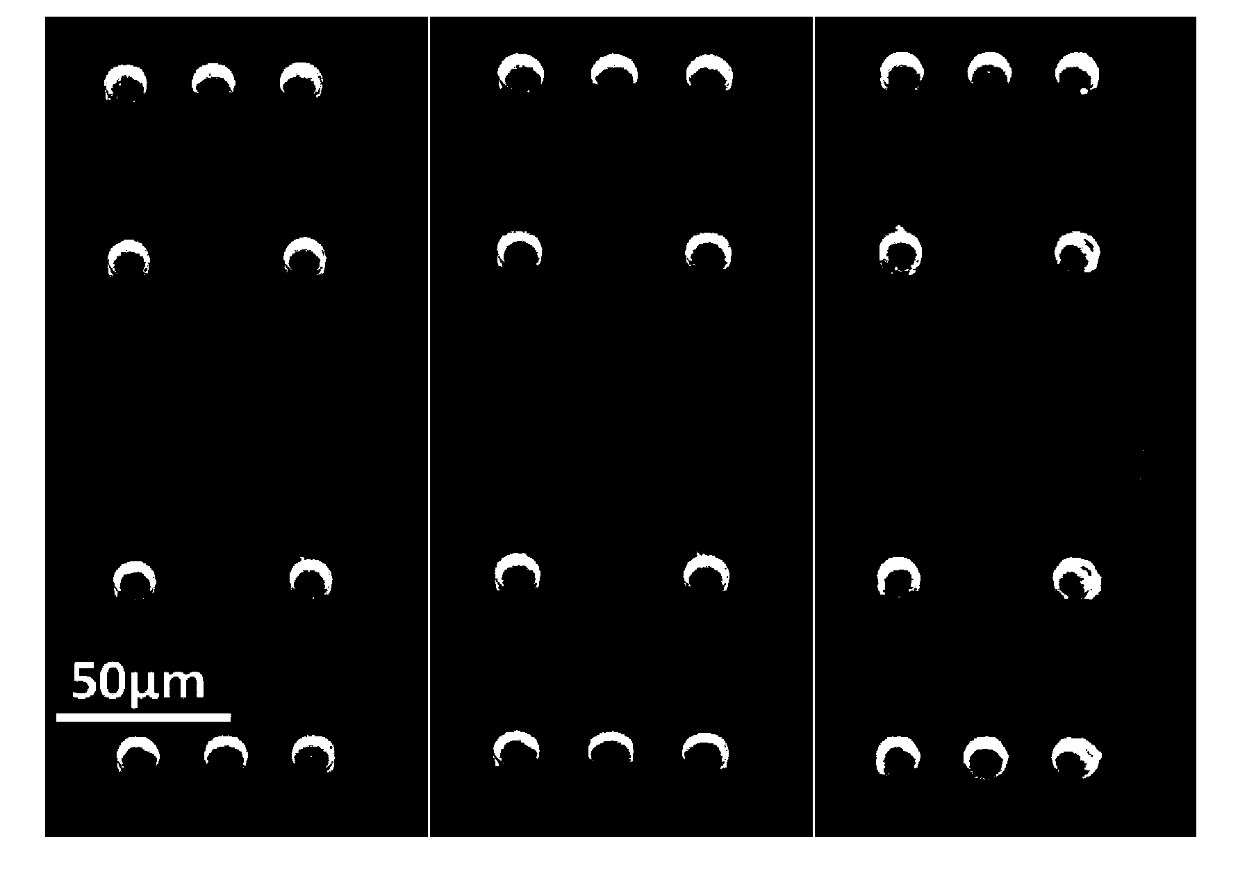
[0047] The micro / nano support array obtained in this embodiment is composed of a substrate and several columnar structures arranged at inter...

Embodiment 2

[0048] Example 2, standard bending strain loading of micro / nano materials

[0049] Using the micro-operating system under the optical microscope, transfer the quasi-one-dimensional target micro / nano material ZnO micro / nano wire to the micro / nano support array prepared in Example 1, so that a single ZnO micro / nano wire (with a diameter of 0.2~ 5.0μm, length 300~800μm) suspended between three or four columnar structures to complete the standard bending strain loading of a single ZnO micro / nanowire;

[0050] The micromanipulation system used consists of a telephoto optical microscope (BX51M, OLYMPUS) and two glass tips controlled by a three-axis hydraulic system (MMO-202ND, OLYMPUS). The ZnO micro / nano wires can be conveniently transferred from the growth substrate to the substrate prepared with micro / nano arrays by real-time observation under a microscope.

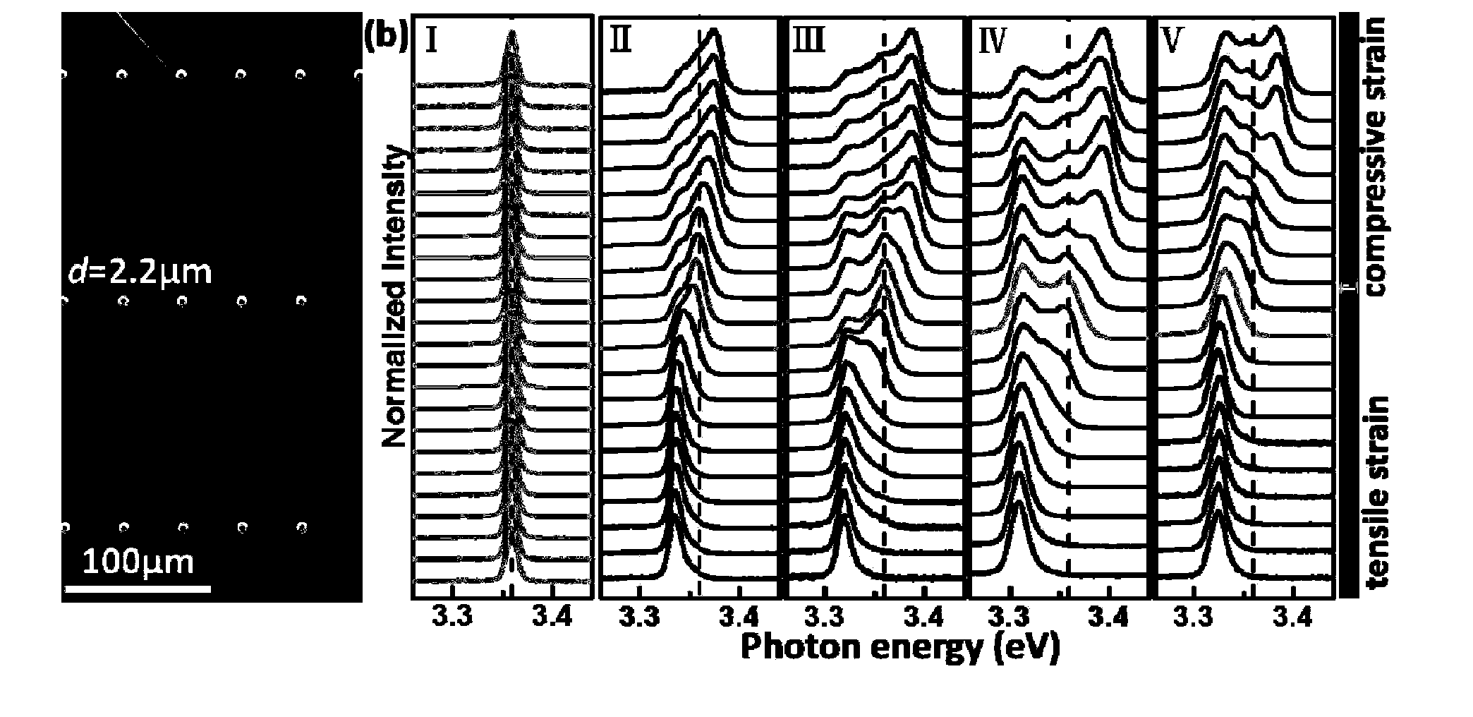
[0051] Perform low-temperature CL spectrum characterization on the cross-section of the standard curved sample to check t...


PUM

PropertyMeasurementUnit
Thicknessaaaaaaaaaa
Diameteraaaaaaaaaa
Diameteraaaaaaaaaa

Abstract

The invention discloses a micro/nano array and application thereof in micro/nano material standard bending strain loading. The micro/nano support array is composed of a substrate and a plurality of column-shaped structures which are located vertically on the substrate and are distributed at intervals to serve as supporting points. A micro/nano supporting dot matrix pattern can be defined freely. The micro/nano array is used for standard bending strain loading of quasi-one-dimensional micro/nano materials with different lengths and thicknesses, and has great application prospects in development of microforce and displacement sensors, flexible micro-nano biology, photoelectric detection and many other aspects.

Description

technical field [0001] The invention relates to a micro / nano array and its application in standard bending strain loading of micro / nano materials. Background technique [0002] The mechanical properties of a material are an important aspect of a nominal material, and strain has a huge impact on the physical properties of the material itself. As early as 1932, the influence of strain on crystal electronics began to cause extensive research. Later, the use of strain to improve semiconductor devices has become an indispensable technology in the semiconductor industry. Especially in the low-dimensional materials that have been developing rapidly recently, such as nanotubes, nanowires, nanofilms and single-layer graphene, etc., the mechanical properties are superior, and the strain has a more significant impact on the physical properties of the material itself. And in many cases, it shows a strong scale-dependent effect (P.W.Bridgman, The effect of homogeneous mechanical stress ...

Claims


Application Information

Patent Timeline
IPC IPC(8): B81B7/04B81C1/00
Inventor 付学文付强朱新利俞大鹏
Owner PEKING UNIV
Why Eureka
Try Eureka