Strain meter using silicon-germanium heterojunction nanowire arrays as sensitive elements and preparation method of strain meter

A silicon-germanium heterojunction and nanowire array technology, which is applied in nanotechnology, nanotechnology, nanotechnology for sensing, etc., can solve the problems of reducing piezoresistive effect and surface state reduction, so as to reduce resistance, Large piezoresistive coefficient and improved sensitivity

Inactive Publication Date: 2014-03-26
SOUTHEAST UNIV
View PDF5 Cites 7 Cited by
  • Summary
  • Abstract
  • Description
  • Claims
  • Application Information

AI Technical Summary

Problems solved by technology

[0003] Although single-component semiconductor nanomaterials also have a larger piezoresistive effect than bulk materials, the surface is usually passivated during the fabrication process, which makes the key factor that causes the giant piezoresistive effect at the nanometer scale - the significant difference in the surface state. reduced, thus greatly reducing the piezoresistive effect

Method used


Image

  • Strain meter using silicon-germanium heterojunction nanowire arrays as sensitive elements and preparation method of strain meter
  • Strain meter using silicon-germanium heterojunction nanowire arrays as sensitive elements and preparation method of strain meter
  • Strain meter using silicon-germanium heterojunction nanowire arrays as sensitive elements and preparation method of strain meter

Examples


preparation example Construction

[0037] The above-mentioned silicon germanium heterojunction nanowire array is used as a method for preparing a strain gauge of a sensitive element, comprising the following steps:

[0038] In the first step, a protective oxide layer is formed on the upper surface of the silicon-on-insulator wafer 1 by a thermal oxidation method, and a silicon-on-insulator wafer with an oxide layer is produced;

[0039]The second step is to open deep grooves: through photolithography and reactive ion etching methods, deep grooves are opened on the silicon-on-insulator wafer with an oxide layer prepared in the first step.

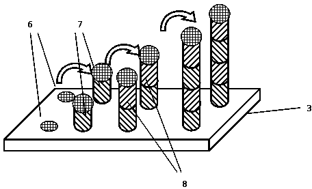
[0040] The second step specifically includes the following processes: step 201), such as Figure 4 As shown, a reactive ion etching process is used to etch and form deep grooves on the silicon-on-insulator wafer 1, so that the silicon layer in the silicon-on-insulator wafer 1 is left with a thickness of 300-500 nanometers; step 202), as Figure 5 As shown, using a thermal ox...

Embodiment

[0050] Utilize above-mentioned preparation method to prepare strain gauge:

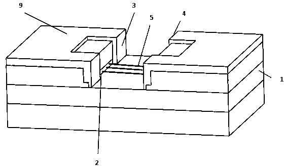
[0051] 1) Prepare SOI substrate: select P-type heavily doped device layer SOI substrate, in which the thickness of the device layer is 1.6 microns, the resistivity is less than 0.1Ω*cm, and the buried oxide layer is 2.0 microns;

[0052] 2) Thermal oxidation: obtain an oxide layer with a thickness of 600 nm on the surface of the SOI substrate;

[0053] 3) Photolithography: remove the oxide layer between the first sidewall 3 and the second sidewall 4;

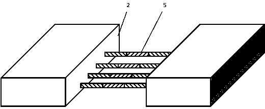
[0054] 4) Reactive ion etching: deep grooves are opened on the SOI substrate. At this time, the device layer is still 400 nanometers thick; the first sidewall 3 and the second sidewall 4 on the SOI substrate are separated by deep grooves ;

[0055] 5) The second thermal oxidation: an oxide layer with a thickness of 200 nanometers is obtained, and the thickness of the device layer is 300 nanometers;

[0056] 6) Photolithography: remove the oxide layer...


PUM

PropertyMeasurementUnit
radiusaaaaaaaaaa
thicknessaaaaaaaaaa
radiusaaaaaaaaaa

Abstract

The invention discloses a strain meter using silicon-germanium heterojunction nanowire arrays as sensitive elements. The strain meter comprises an silicon-on-insulator wafer and an oxide layer covering the silicon-on-insulator wafer. A deep groove is formed in the silicon-on-insulator wafer. The oxide layer is disposed on both the side wall and the bottom of the deep groove. Two windows for growing nanowire are respectively formed in the two opposite side walls of the deep groove. A tin nano-particle catalyst layer is disposed on each window. One silicon-germanium heterojunction nanowire array grows on each tin nano-particle catalyst layer. The two opposite windows are connected through the silicon-germanium heterojunction nanowire arrays. The strain meter using the silicon-germanium heterojunction nanowire arrays as the sensitive elements has the advantages that the sensitivity of sensitivity sources is increased. In the mean time, the invention further discloses a preparation method of the strain meter, and the preparation method is simple and compatible with the existing integrated circuit processes.

Description

technical field [0001] The invention relates to a nano-electro-mechanical system (abbreviation: NEMS) sensor sensitive element, in particular to a strain gauge with a silicon-germanium heterojunction nanowire array as a sensitive element and a preparation method thereof. Background technique [0002] Nanowires, especially nanowires of semiconductor materials, have attracted the attention of scientists due to the importance of silicon and germanium materials in today's integrated circuit field, and the compatibility of preparation processes with mature microelectronics processes. At present, nanowires of various materials have huge application space in different fields, such as light-emitting diodes (LEDs), solar energy, sensors and other fields. At the same time, the development of nanoelectromechanical systems (NEMS) technology has greatly reduced the size of pressure sensors. At the same time, due to the confinement effect at the nanoscale, nanomaterials as sensitive sourc...

Claims


Application Information

Patent Timeline
Patent Type & Authority Applications(China)
IPC IPC(8): G01B7/16B82Y15/00B82Y40/00
Inventor 雷双瑛李峄陈洁于虹黄庆安
Owner SOUTHEAST UNIV
Why Eureka
Try Eureka