Silicide Formation Method

A technology of silicide and chemical vapor deposition, which is applied in the manufacture of electrical components, semiconductor/solid-state devices, circuits, etc., can solve the problems of increased contact resistance and sheet resistance, decreased operating speed of semiconductor devices, and small contact areas, etc., to achieve uniform width , improve performance, uniform deposition thickness

Active Publication Date: 2016-08-03
SEMICON MFG INT (SHANGHAI) CORP
View PDF10 Cites 0 Cited by
  • Summary
  • Abstract
  • Description
  • Claims
  • Application Information

AI Technical Summary

Problems solved by technology

However, contact resistance and sheet resistance increase due to the small gate and source / drain contact areas formed in sub-micron MOS devices
This makes the operating speed of semiconductor devices greatly reduced

Method used


Image

  • Silicide Formation Method
  • Silicide Formation Method
  • Silicide Formation Method

Examples


Embodiment Construction

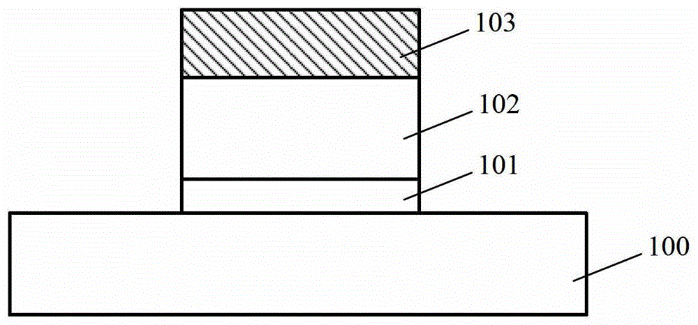
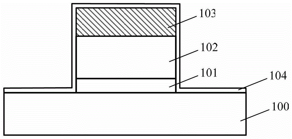
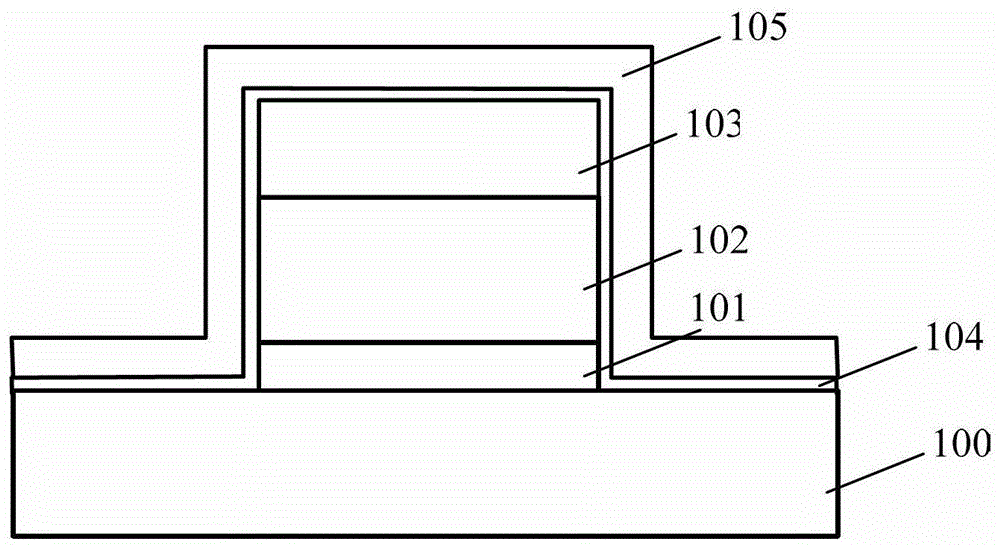
[0031] As described in the background art, in the prior art, forming silicide on the gate electrode layer can reduce the resistance of the gate electrode to a certain extent, but as the size of the gate electrode layer is further reduced, the resistance of the gate electrode layer further increases.

[0032] It was found that the gate electrode layer resistance increases with decreasing device size as the gate length becomes shorter and narrower gate lines have higher sheet resistance than wider gate lines due to edge effects. And increasing the surface area of ​​the gate electrode layer can reduce the resistance of the gate electrode layer.

[0033] To this end, embodiments of the present invention disclose a method for forming a silicide. The method for forming a silicide increases the area of ​​a gate electrode layer, and then forms a silicide layer on this basis, thereby effectively reducing the resistance of the gate electrode layer. .

[0034] The technical solutions of...


PUM


Abstract

A formation method of silicide is provided. The formation method includes the following steps that: a substrate is provided; side walls are formed at two sides of a gate dielectric layer, a gate electrode layer and a first mask layer at the surface of the substrate; first sacrificial layers are formed on the surface of the substrate; the first mask layer is removed, grooves are formed between the top surface of the gate electrode layer and the side walls; a second sacrificial layer coating the top surface of the gate electrode layer and groove side walls is formed in the grooves, and the width of the second sacrificial layer located at the groove side walls is uniform; a second mask layer is formed on the surface of the second sacrificial layer, and the grooves are filled with the second mask layer; with the second mask layer adopted as a mask, the second sacrifice layer and the gate electrode layer are etched until part of the gate electrode layer with a certain thickness is removed; and a silicide layer is formed on the surface of the gate electrode layer of which part with a certain thickness is removed. With the formation method of the silicide adopted, the superficial area of the formed gate electrode layer is increased, and the degradation of the resistance of the gate electrode layer can be benefitted, and operating rate of a device can be improved.

Description

technical field [0001] The present invention relates to the technical field of semiconductors, and in particular, to a method for forming silicide. Background technique [0002] With the continuous development of CMOS technology, sub-micron devices have been widely used. However, due to the fine gate and source / drain contact regions formed in sub-micron MOS devices, the contact resistance and sheet resistance increase. This greatly reduces the operating speed of semiconductor devices. [0003] The salicide formation process can effectively reduce sheet resistance and contact resistance by forming silicide in the gate and source / drain regions. The formation process of self-aligned silicide in the prior art is mainly to form a metal layer on the surface of polysilicon through evaporation or sputtering process; annealing treatment, the metal reacts with polysilicon to form metal silicide; and the unreacted metal layer is removed. [0004] For more information on the formatio...

Claims


Application Information

Patent Timeline
Patent Type & Authority Patents(China)
IPC IPC(8): H01L21/283H01L21/285
CPCH01L21/28052
Inventor 隋运奇韩秋华
Owner SEMICON MFG INT (SHANGHAI) CORP
Why Eureka
Try Eureka