Preparation method of TEM sample

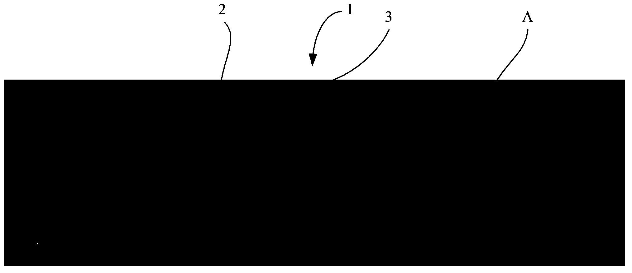
A sample and focused ion beam technology, which is applied in the field of semiconductor device manufacturing, can solve the problems of inaccurate measurement of the height of the high dielectric layer 5, ghosting (overlap, TEM samples are prone to damage, etc.), and achieve fast fixed-point sample preparation and solve damage , the effect of solving adverse effects

Active Publication Date: 2014-04-02
SEMICON MFG INT (SHANGHAI) CORP
View PDF10 Cites 11 Cited by
  • Summary
  • Abstract
  • Description
  • Claims
  • Application Information

AI Technical Summary

Problems solved by technology

[0003] Sample preparation is a very important part of TEM analysis technology. There are usually two methods for sample preparation in the prior art. One of the methods is to cut the primary sample from the wafer by cutting, and then the primary sample is mechanically polished (polishing) Then put it into the PIPS machine (Precision ion polishing system) to perform ion milling on the primary sample to form a TEM sample. The TEM sample prepared by this method is relatively thin, and the front and rear imaging end faces of the TEM sample are very amorphous. less, it will not affect the imaging quality, and has higher resolution, but this method takes a long time and is not suitable for sample preparation at a fixed point; there is another method that uses a Focused Ion Beam (FIB) machine The sample is obtained by cutting, and the preparation of the TEM sample can be completed in a local area of ​​the entire wafer. The process is to use a high-voltage accelerated ion beam to focus on a local area of ​​the wafer, thereby directly cutting the wafer to obtain a TEM sample. Figure 1a and Figure 1b Shows the scanning images of wafer TEM samples formed with high dielectric layer transistors prepared using focused ion beams, such as Figure 1a As shown, a plurality of high dielectric layer transistors 2 are formed on the wafer 1, and STI (Shallow Trench Isolation) regions 3 are formed between the high dielectric layer transistors 2, and the target region A is cut with a focused ion beam to get as Figure 1b Imaged end face of sample shown
[0004] Due to the use of high-voltage accelerated ion beams for bombardment, it is easy to cause damage to the TEM sample, so that the front and rear imaging end faces of the TEM sample in the thickness direction change from crystalline to amorphous, which affects the imaging quality; and, due to technical limitations , when using focused ion beams to prepare samples, the thickness of the target region A is generally in the range of 80-100nm. With the development of semiconductor technology, the feature size of semiconductor devices has been reduced to 45nm or even smaller. Therefore, the The thickness of the TEM sample is larger than the feature size of the device, and the thicker TEM sample is easy to cause the overlap phenomenon when imaging, such as Figure 1c As shown, still taking the high dielectric transistor as an example, when the thickness of the TEM sample is larger than the feature size of the device, such as Figure 1a In the shown target area A, there will be a part of the morphology of the undesired STI area 3 remaining in the TEM sample. When the undesired STI area 3 exists too much, and due to the high dielectric The electrical layer is higher than the thickness of the high dielectric layer 5 in the active region of the transistor 2, and a ghost image 6 is formed during imaging, thereby making the height of the gate 4 of the high dielectric layer transistor 2 and the height of the high dielectric layer 5 cannot be measured accurately

Method used


Image

  • Preparation method of TEM sample
  • Preparation method of TEM sample
  • Preparation method of TEM sample

Examples


Embodiment Construction

[0022] The principles and features of the present invention are described below in conjunction with the accompanying drawings, and the examples given are only used to explain the present invention, and are not intended to limit the scope of the present invention.

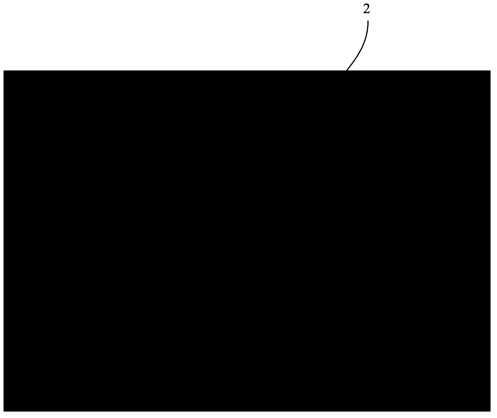
[0023] As a typical embodiment of a TEM sample preparation method of the present invention, such as figure 2 shown, including:

[0024] Cut a primary sample from the wafer by dicing and laser mark the cut primary sample to designate the target area;

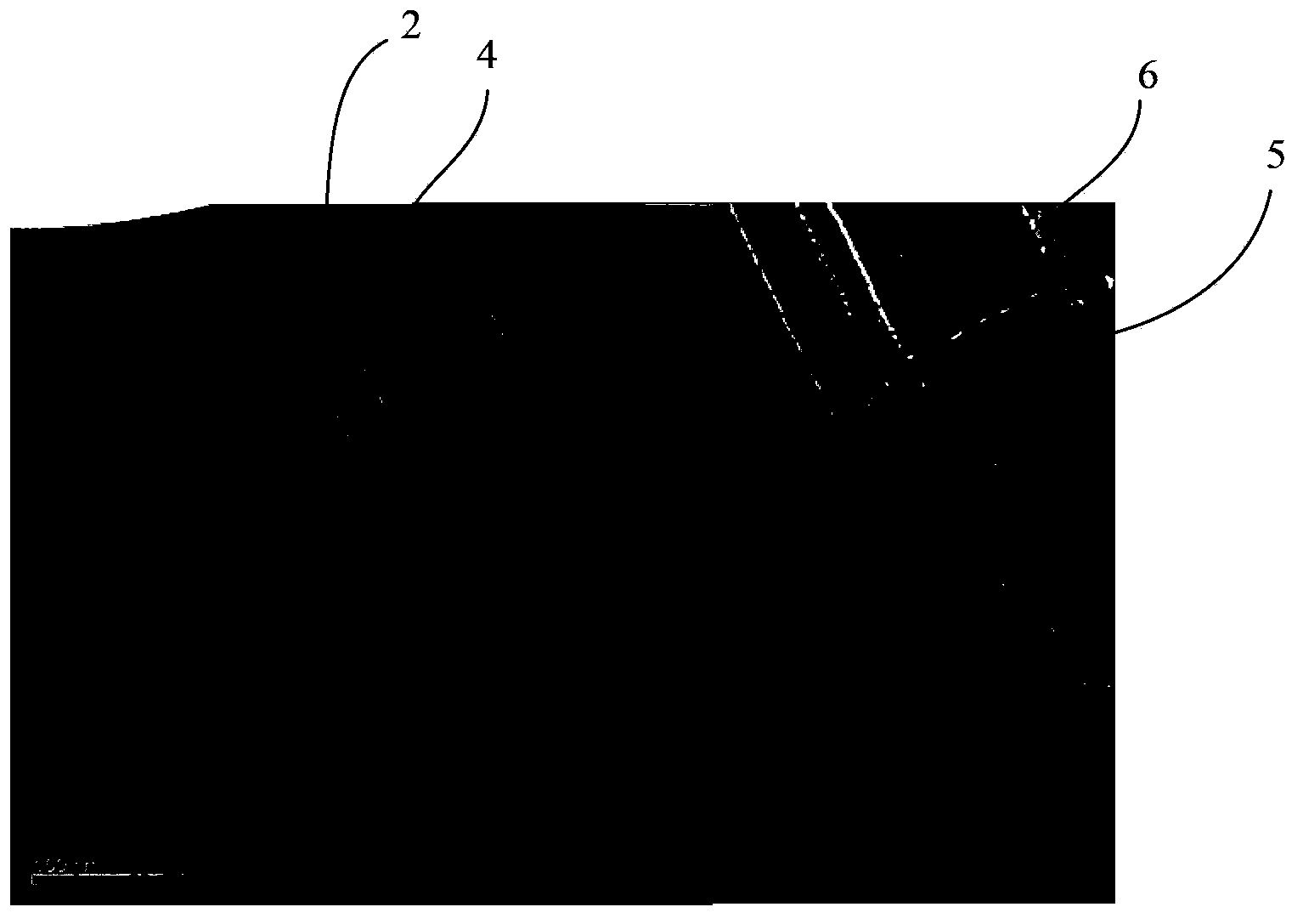
[0025] Put the primary sample into the focused plasma machine and perform focused ion beam cutting on the designated target area to obtain a sample with front and rear imaging end faces in the thickness direction;

[0026] The step of performing ion thinning on the sample cut by the focused ion beam, which includes: adhering the sample cut by the focused ion beam to a support, wherein a part of an imaging end surface of the sample cut by the focused ion beam and the ...


PUM

PropertyMeasurementUnit
thicknessaaaaaaaaaa

Abstract

The invention discloses a preparation method of a TEM sample. The method combines the advantages of ion milling and focused ion beam methods used in the prior art. The sample of a designated area can be obtained by a focused ion beam, thus saving the time needed by polishing in the prior art and realizing fixed-point sample preparation. An amorphous layer at an imaging end face is removed by ion milling so as to solve the damage of the focused ion beam on the imaging end face and further decrease the thickness of the TEM sample, thus avoiding the overlap phenomenon. Thus, the preparation method of a TEM sample provided by the invention can realize rapid fixed-point sample preparation, and at the same time solves the problem that the amorphous end face and overlap can generate adverse effects on imaging during cutting.

Description

technical field [0001] The invention relates to the technical field of semiconductor device manufacturing, in particular to a method for preparing a TEM (Transmission Electron Microscope, transmission electron microscope) sample. Background technique [0002] In the semiconductor manufacturing industry, there are a variety of inspection equipment, among which the electron microscope is an important tool for inspecting the morphology, size and characteristics of the thin film during composition. Commonly used electron microscopes include TEM (Transmission Electron Microscope, transmission electron microscope) and SEM (Scanning Electron Microscope, scanning electron microscope). The working principle of TEM is to put the sample to be detected into the TEM observation room, irradiate the sample with a high-voltage accelerated electron beam, enlarge the sample shape, project it on the screen, take a picture, and then analyze it. One of the outstanding advantages of TEM is that i...

Claims


Application Information

Patent Timeline
Patent Type & Authority Applications(China)
IPC IPC(8): G01N1/28
Inventor 齐瑞娟赵燕丽段淑卿陈柳
Owner SEMICON MFG INT (SHANGHAI) CORP
Why Eureka
Try Eureka