Method for preparing SiC ohmic contact by ultraviolet pulse laser irradiation device

A technology of pulsed laser and ohmic contact, which is applied in semiconductor/solid-state device manufacturing, electrical components, semiconductor devices, etc., can solve unseen problems and achieve the effects of short processing time, precise processing range, and control processing range

Inactive Publication Date: 2014-04-02
SHANGHAI NORMAL UNIVERSITY
View PDF3 Cites 8 Cited by
  • Summary
  • Abstract
  • Description
  • Claims
  • Application Information

AI Technical Summary

Problems solved by technology

For example, a published patent related to a laser-induced GaNP-type ohmic contact preparation method, but there is no report on its application on SiC

Method used


Image

  • Method for preparing SiC ohmic contact by ultraviolet pulse laser irradiation device
  • Method for preparing SiC ohmic contact by ultraviolet pulse laser irradiation device

Examples


Embodiment 1

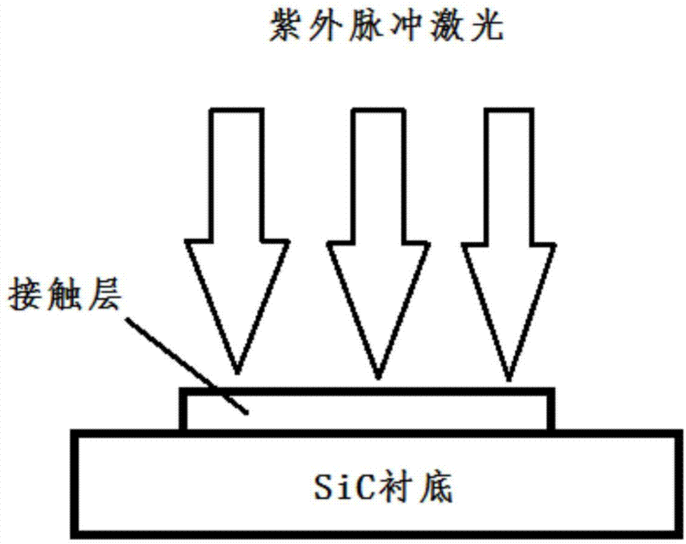
[0015] Embodiment 1 (as attached figure 1 shown)

[0016] The n-type 4H-SiC is used as the substrate, the surface of the substrate is cleaned, and a layer of Ni metal is sputtered by a magnetron sputtering method. Using a focused pulsed laser with a wavelength of 248nm and a single pulse energy of 250mJ, the front side of the above material is irradiated in an argon atmosphere to obtain an ohmic contact.

Embodiment 2

[0018] The n-type 4H-SiC is used as the substrate, the surface of the substrate is cleaned, and a layer of Ti metal is sputtered by magnetron sputtering. Using a focused pulsed laser with a wavelength of 248nm and a single pulse energy of 250mJ, the front side of the above material is irradiated in an argon atmosphere to obtain an ohmic contact.

Embodiment 3

[0020] The n-type 4H-SiC is used as the substrate, the surface of the substrate is cleaned, and a layer of Ni metal is sputtered by a magnetron sputtering method. A pulsed laser with a wavelength of 248nm and a single pulse energy of 300mJ is used to focus and irradiate the front side of the above material in an argon atmosphere to obtain an ohmic contact.


PUM


Abstract

The invention discloses a method for preparing a SiC ohmic contact by an ultraviolet pulse laser irradiation device, and relates to the technical field of semiconductor device preparation. The method comprises the following steps of cleaning the surface of a SiC substrate; preparing a contact layer on the SiC surface; after ultraviolet pulse lasers are focused, irradiating the front of the material under the condition of high vacuum or under the protection of inert gas to obtain the ohmic contact. The ultraviolet pulse laser irradiation replaces the traditional thermal annealing, and the SiC ohmic contact with high performance can be obtained. Compared with the traditional thermal annealing, the method has the advantages of short processing time and high reaction temperature, and the range of a processing area can be accurately controlled.

Description

technical field [0001] The invention relates to the technical field of semiconductor device preparation, in particular to a method for preparing SiC ohmic contacts by ultraviolet pulsed laser irradiation. Background technique [0002] In the development of semiconductor materials, Si and Ge are generally called the first-generation electronic materials, GaAs, GaP, InP, etc. are called the second-generation electronic materials, and wide-bandgap semiconductors SiC, C-BN (cubic boron nitride ), GaN, ZnSe, and diamond thin films are called third-generation semiconductor materials. In the field of semiconductor devices, a key process issue is the preparation of ohmic contacts. [0003] Ohmic contact plays an important role in the signal transmission between semiconductors and external circuits, and its quality directly affects performance indicators such as device efficiency, gain, and switching speed. Poor ohmic contact limits the working performance and stability of the devic...

Claims


Application Information

Patent Timeline
Patent Type & Authority Applications(China)
IPC IPC(8): H01L21/28H01L21/268
CPCH01L21/28506H01L21/268
Inventor 卢吴越张永平程越谈嘉慧赵高杰刘益宏孙玉俊陈之战石旺舟
Owner SHANGHAI NORMAL UNIVERSITY
Why Eureka
Try Eureka