Method of laser separation of the epitaxial film or of the epitaxial film layer from the growth substrate of the epitaxial semiconductor structure (variations)

A technology of epitaxial structure and growth substrate, which is applied in the field of laser processing and can solve problems such as inapplicability

Active Publication Date: 2014-04-02
尤里·杰奥尔杰维奇·施赖特尔 +2
View PDF7 Cites 11 Cited by
  • Summary
  • Abstract
  • Description
  • Claims
  • Application Information

AI Technical Summary

Problems solved by technology

In this case, the growth substrate and the epitaxial film have equal gap widths,

Method used


Image

  • Method of laser separation of the epitaxial film or of the epitaxial film layer from the growth substrate of the epitaxial semiconductor structure (variations)
  • Method of laser separation of the epitaxial film or of the epitaxial film layer from the growth substrate of the epitaxial semiconductor structure (variations)
  • Method of laser separation of the epitaxial film or of the epitaxial film layer from the growth substrate of the epitaxial semiconductor structure (variations)

Examples


Embodiment 1

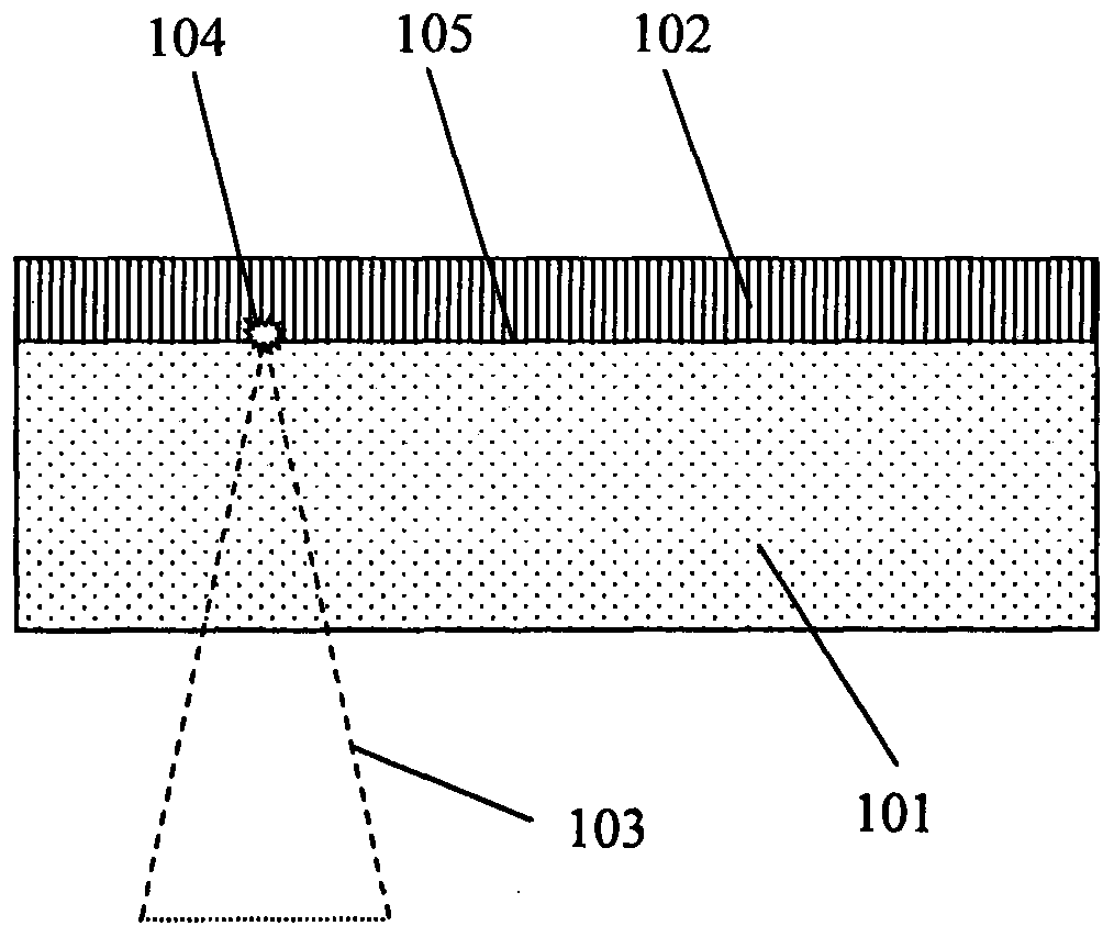
[0033] Example 1. A homoepitaxial gallium nitride film doped with a fine donor impurity is separated from an undoped semiconductor gallium nitride substrate by passing a laser beam through the substrate.

[0034] figure 2 A scheme for laser separation of a homoepitaxial GaN film 202 (50 μm wide) from a semiconductor GaN substrate 101 (200 μm wide) is shown. The doping level of fine silicon donor impurities in the homoepitaxial film 202 is 5×10 19 cm -3 , and greater than fine oxygen and silicon donors equal to 10 in the semiconductor substrate 101 17 cm -3 background density.

[0035] To separate homoepitaxial GaN films, CO 2 Pulse pumped laser, operating at wavelength λ = 10.6 μm and generating pulses with energy 0.1 J, duration 50 ns and repetition rate 100 Hz.

[0036] Laser radiation having a wavelength λ=10 μm at a concentration of 5×10 19 cm -3 The absorption coefficient in the fine silicon donor impurity-doped homoepitaxial GaN film 202 is equal to 4×10 4 cm ...

Embodiment 2

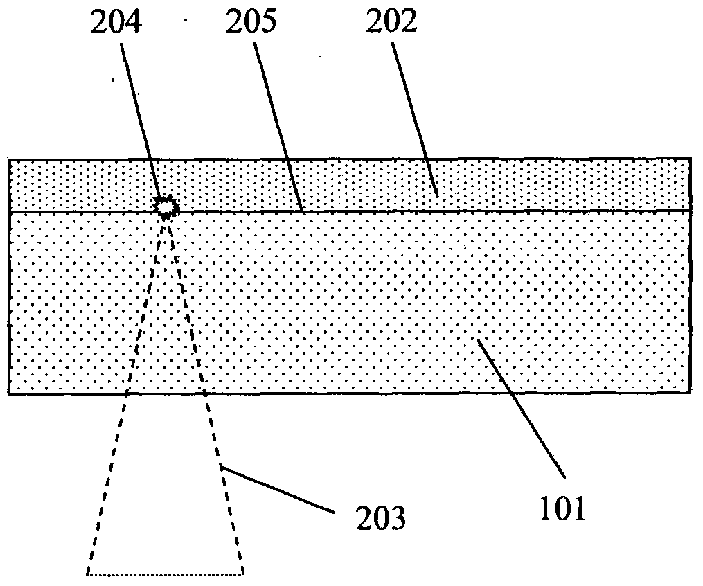
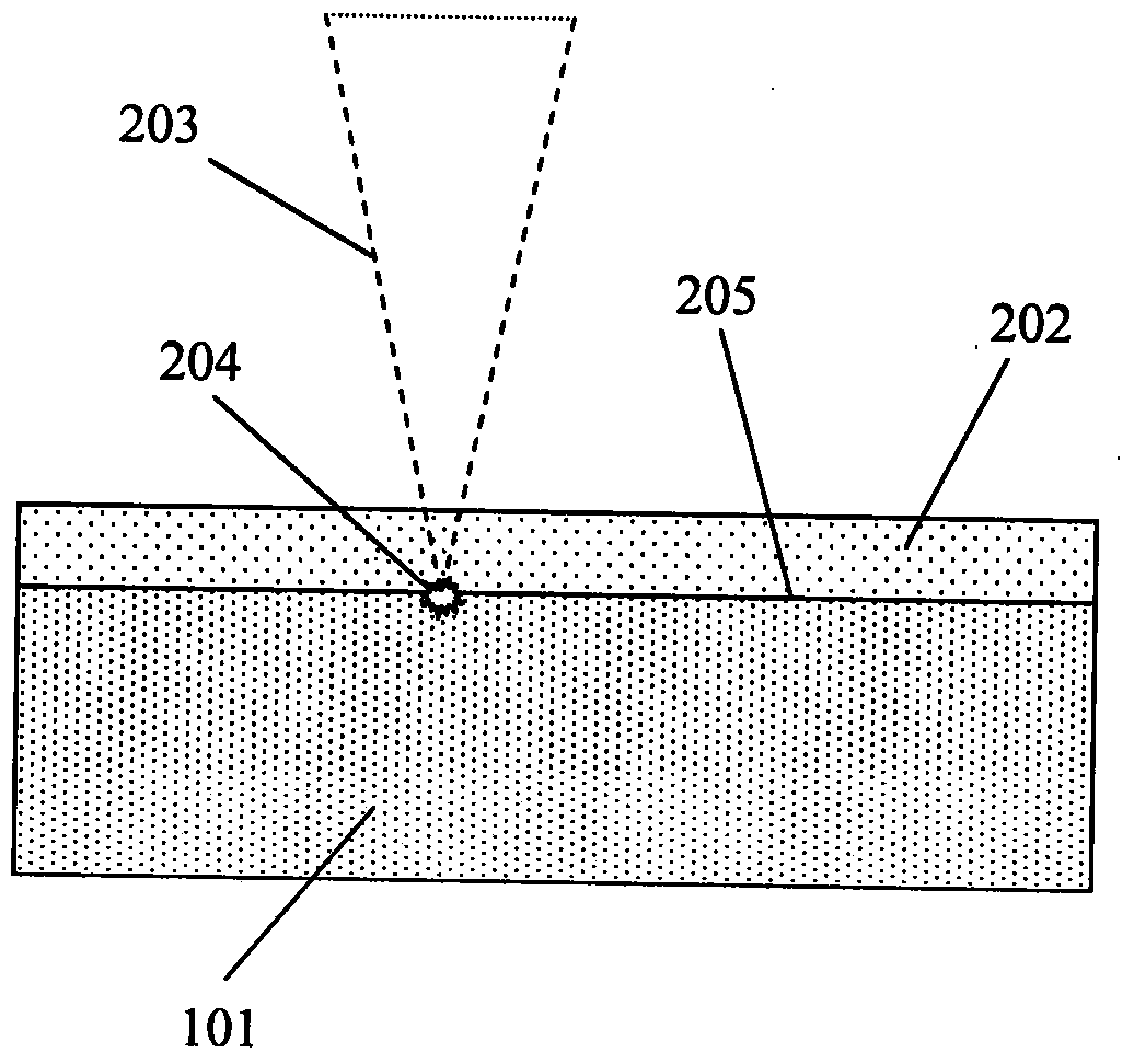
[0039] Example 2. Separation of an undoped homoepitaxial gallium nitride film from a semiconductor gallium nitride substrate doped with fine donor impurities by means of a laser beam passing through the homoepitaxial film.

[0040] image 3 A scheme for laser separation of an undoped 100 μm thick homoepitaxial GaN film from a 1 mm thick semiconducting GaN substrate is shown. The background concentration of fine oxygen and silicon donors in the homoepitaxial film 202 is 10 17 cm -3 and substantially less than the concentration of fine silicon donor impurities in the doped semiconductor substrate 101 (equal to 5×10 19 cm -3 ).

[0041] To separate homoepitaxial GaN films, CO 2 A pulsed pump laser operating at wavelength λ=10.6 μm and generating pulses of energy 0.1 J, duration 50 ns and repetition rate 100 Hz. Laser radiation having a wavelength λ=10 μm at a wavelength equal to 10 17 cm -3 The absorption coefficient of the undoped homoepitaxial GaN film 202 at a backgrou...

Embodiment 3

[0044] Example 3. Separation of the undoped upper layer of a homoepitaxial GaN film from an undoped semiconductor GaN substrate, where a laser beam passes through the substrate and is absorbed into the homoepitaxial layer doped with fine donor impurities. lower layer of the membrane. Figure 4 A scheme is shown for laser separation of a 50 μm thick undoped homoepitaxial GaN film 202 from a 200 μm thick undoped semiconductor GaN substrate 101 using a doped underlayer 406 of a 1 μm thick homoepitaxial film . The doping level of the fine silicon donor impurity in the lower layer 406 of the homoepitaxial GaN film is 5×10 19 cm -3 And greater than the background concentration of fine silicon and oxygen donor impurities in the semiconductor substrate 101 and the upper layer of the homoepitaxial film 202 (equal to 10 17 cm -3 ).

[0045] To separate homoepitaxial GaN films, CO 2 A pulsed pump laser operating at wavelength λ=10.6 μm and generating pulses of energy 0.1 J, duratio...


PUM

PropertyMeasurementUnit
Absorption coefficientaaaaaaaaaa

Abstract

The present invention proposes variations of the laser separation method allowing separating homoepitaxial films from the substrates made from the same crystalline material as the epitaxial film. This new method of laser separation is based on using the selective doping of the substrate and epitaxial film with fine donor and acceptor impurities. In selective doping,, concentration of free carries in the epitaxial film and substrate may essentially differ and this can lead to strong difference between the light absorption factors in the infrared region near the residual beams region where free carriers and phonon-plasmon interaction of the optical phonons with free carriers make an essential contribution to infrared absorption of the optical phonons. With the appropriate selection of the doping levels and frequency of infrared laser radiation it is possible to achieve that laser radiation is absorbed in general in the region of strong doping near the interface substrate- homoepitaxial film. When scanning the interface substrate- homoepitaxial film with the focused laser beam of sufficient power, thermal decomposition of the semiconductor crystal takes place with subsequent separation of the homoepitaxial film. The advantage of the proposed variations of the method for laser separation of epitaxial films in comparison with the known ones is in that it allows to separate homoepitaxial films from the substrates, i.e., homoepitaxial films having the same width of the forbidden gap as the initial semiconductor substrate has. The proposed variations of the method can be used for separation of the epitaxial films. Besides, the proposed method allows using the high-effective and inexpensive infrared gas silicon dioxide CO2 or silicon oxide CO lasers for separation of the epitaxial films.

Description

technical field [0001] The group of the invention relates to laser treatment of solid materials, in particular to methods of separating surface layers of semiconductors using laser radiation, ie methods of laser separating epitaxial films or layers of epitaxial films from epitaxial semiconductor structures. Background technique [0002] According to the flip-chip technology, the epitaxial layer of the semiconductor crystal is transferred to the non-growth substrate and the epitaxial layer of the semiconductor crystal is separated from the growth substrate by laser. In the manufacture of diodes (US6365429). [0003] Laser separation of gallium nitride layers from transparent grown sapphire substrates was proposed for the first time in Kelly et al., Physica Status Solidi (a) vol. 159, pp. R3, R4, (1997). In this work, a ratio with satisfaction is used Ultraviolet excimer laser (ultraviolet excimer laser) with wavelength λ=355nm, for this laser, its quantum energy is in the ...

Claims


Application Information

Patent Timeline
IPC IPC(8): H01L21/762
CPCH01L21/76254H01L33/0079H01L21/02518H01L33/0093H01L21/02527H01L21/02529H01L21/02532H01L21/0254H01L21/02546H01L21/02551H01L21/0257H01L21/02634H01L21/268H01L21/6835H01L2221/68381
Inventor 尤里·杰奥尔杰维奇·施赖特尔尤里·托马索维奇·列巴涅阿列克谢·弗拉基米罗维奇·米罗诺夫
Owner 尤里·杰奥尔杰维奇·施赖特尔
Why Eureka
Try Eureka