Substrate for power module, substrate for power module with heat sink, power module, and method for manufacturing substrate for power module

A technology for power modules and substrates, which is used in the improvement of metal adhesion of insulating substrates, manufacturing tools, circuit substrate materials, etc., and can solve the problems of cracking of insulating substrates and inability to fully alleviate thermal deformation.

Active Publication Date: 2014-04-16
MITSUBISHI MATERIALS CORP
View PDF10 Cites 4 Cited by
  • Summary
  • Abstract
  • Description
  • Claims
  • Application Information

AI Technical Summary

Problems solved by technology

Therefore, the copper plate cannot sufficiently relax the thermal deformation caused by the difference in the thermal expansion coefficient between the hea...

Method used


Image

  • Substrate for power module, substrate for power module with heat sink, power module, and method for manufacturing substrate for power module
  • Substrate for power module, substrate for power module with heat sink, power module, and method for manufacturing substrate for power module
  • Substrate for power module, substrate for power module with heat sink, power module, and method for manufacturing substrate for power module

Examples


Embodiment 1

[0248] A comparative experiment performed to confirm the effectiveness of the present invention will be described.

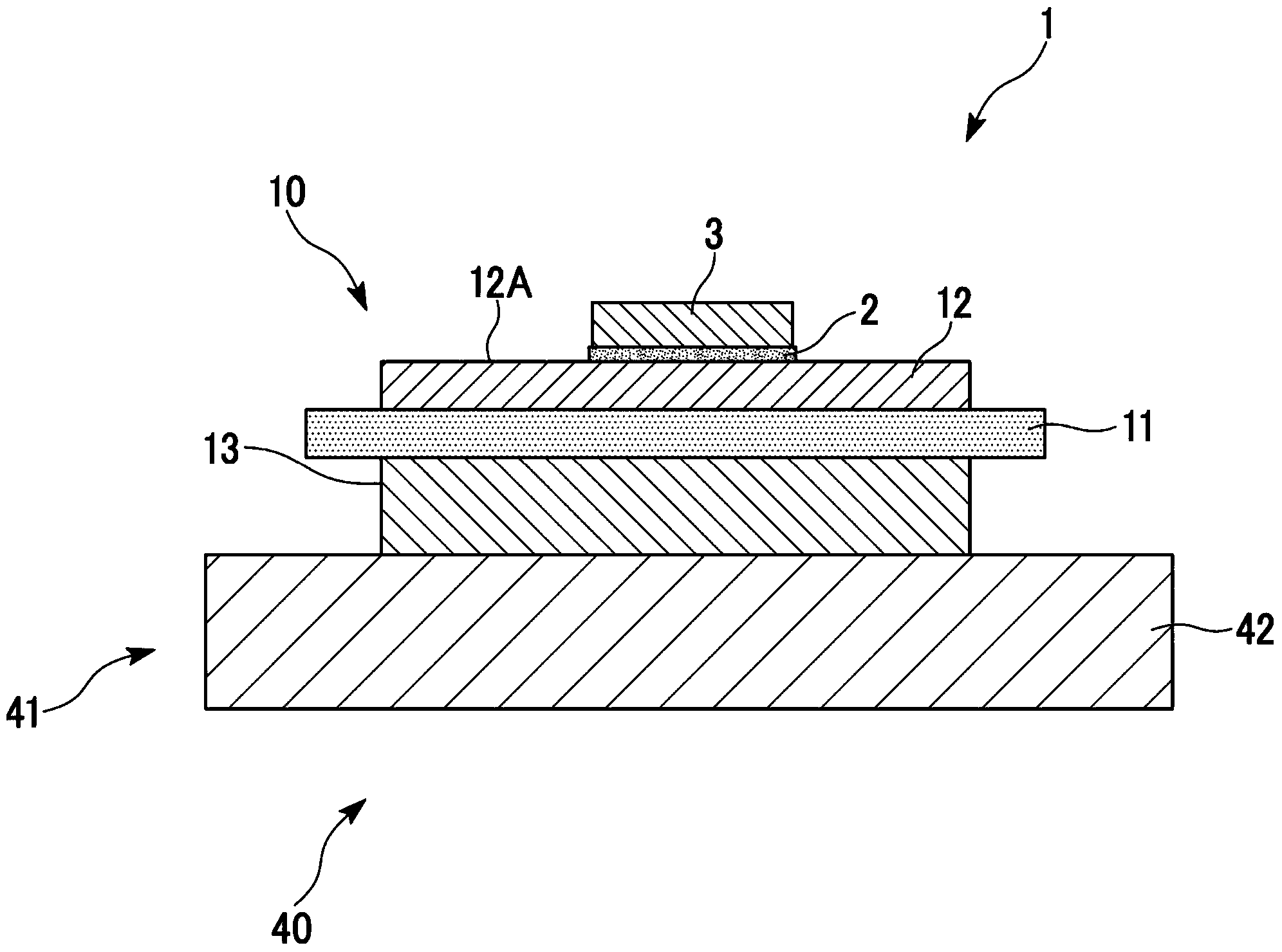
[0249] Prepare a ceramic substrate made of AlN with a thickness of 0.635mm, and a ceramic substrate with a thickness of 0.3mm made of doped copper, oxygen-free copper (OFC) and tough copper (TPC) with the composition shown in Table 1. A copper plate, and an aluminum plate with a thickness of 1.6 mm made of aluminum (4NAl) with a purity of 99.99% by mass.

[0250] These ceramic substrates, copper plates, and aluminum plates are joined by the method described in the third embodiment. Set the pressing pressure in the circuit layer forming step S201 to 0.5 gf / cm 2 , Set the heating temperature to 850°C. In addition, the pressing pressure in the first metal layer forming step S202 was set to 5 kgf / cm 2 , and set the heating temperature to 640°C.

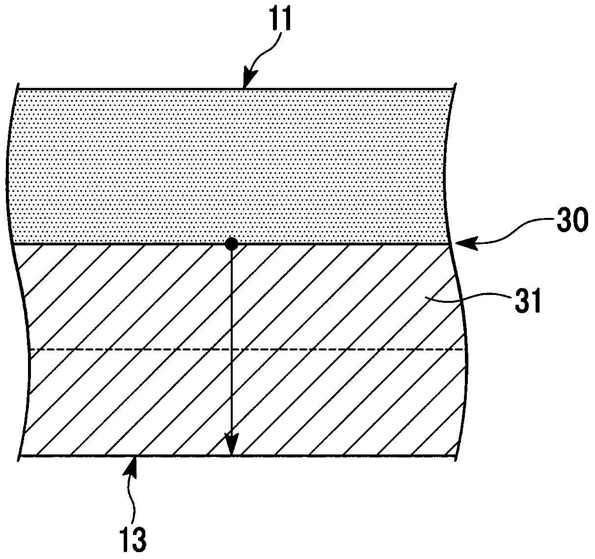
[0251] These substrates for power modules were subjected to a predetermined number of cooling and heating cycles (-40...

Embodiment 2

[0258] A comparative experiment conducted to confirm the effectiveness of the present invention will be described.

[0259] Prepared by Al 2 o 3 A ceramic substrate with a thickness of 0.635 mm and a copper plate with a thickness of 0.3 mm composed of copper or a copper alloy having the compositions shown in Table 2 were used.

[0260] These copper plates, ceramic substrates, and copper plates are joined by the method described in the seventh embodiment. The pressing pressure in the circuit layer forming step S601 and the second metal layer forming step S602 is set to 0.5kgf / cm 2 , and set the heating temperature to 850°C.

[0261] These substrates for power modules were subjected to a predetermined number of cooling and heating cycles (-40°C to 110°C and 110°C to -40°C) to check for cracks in the ceramic substrate.

[0262] [Table 2]

[0263]

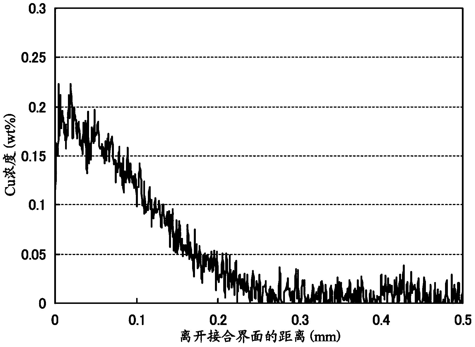
[0264] In the conventional example B1 using ductile copper and the conventional example B2 using oxygen-free copper (OFC), crac...


PUM


Abstract

This substrate (10) for a power module is provided with an insulating substrate (11) and a circuit layer (12) formed on one surface of the insulating substrate (11). The circuit layer (12) is configured by bonding a first copper plate (22) onto one surface of the insulating substrate (11). Before being bonded, the first copper plate (22) has a composition containing at least: a total of 1 molppm to 100 molppm of one or more of an alkali earth metal, a transition metal element, and a rare earth element; or 100 molppm to 1000 molppm of boron; with the remainder being copper and unavoidable impurities.

Description

technical field [0001] The present invention relates to a substrate for a power module, a substrate for a power module with a heat sink, a power module, and a method for manufacturing a substrate for a power module used in semiconductor devices that control large current and high voltage. [0002] This application claims priority based on Japanese Patent Application No. 2011-176712 and Japanese Patent Application No. 2011-176881 filed in Japan on Aug. 12, 2011, and the contents thereof are incorporated herein by reference. Background technique [0003] Among semiconductor elements, a power module for supplying electric power has a relatively high calorific value. Therefore, as a substrate on which the power module is mounted, for example, a substrate for a power module is used, which includes: AlN (aluminum nitride), Al 2 o 3 (alumina), Si 3 N 4 (silicon nitride) or the like; a circuit layer having a first metal plate bonded to one side of the insulating substrate; and a ...

Claims


Application Information

Patent Timeline
IPC IPC(8): H01L23/13H01L23/36H05K1/02H05K1/05
CPCH05K3/0061H01L23/3735H05K1/09H05K1/0204H05K3/38H05K3/103H05K1/0306H01L23/3736H01L2224/32225H01L24/29H01L24/32H01L24/83H01L2224/29111H01L2224/83455C04B35/645C04B37/021C04B37/025C04B37/026C04B2237/064C04B2237/121C04B2237/124C04B2237/125C04B2237/127C04B2237/343C04B2237/366C04B2237/402C04B2237/407C04B2237/54C04B2237/60C04B2237/704C04B2237/706C04B2237/708C04B2237/86H01L2924/01322B23K35/262B23K35/3006B23K35/0222B23K35/0233B23K35/0238C22C9/00C22C13/00C22C21/00Y10T29/49155H01L2924/01047H01L2924/01049H01L2924/01029H01L2924/00
Inventor 黑光祥郎长友义幸寺崎伸幸坂本敏夫牧一诚森广行荒井公
Owner MITSUBISHI MATERIALS CORP
Why Eureka
Try Eureka