Composite drain-based AlGaN/GaN MIS-HEMT (Metal-Insulator-Semiconductor High-Electron-Mobility Transistor) high-voltage device and fabrication method thereof

A composite drain and high-voltage device technology, applied in the field of microelectronics, can solve problems such as large on-resistance, achieve the effects of improving breakdown voltage, avoiding gate leakage current, good controllability and repeatability

Inactive Publication Date: 2014-04-23
XIDIAN UNIV
View PDF4 Cites 6 Cited by
  • Summary
  • Abstract
  • Description
  • Claims
  • Application Information

AI Technical Summary

Problems solved by technology

[0007] However, the high-voltage devices with the above two structures all have the disadvantage of large on-resistance

Method used


Image

  • Composite drain-based AlGaN/GaN MIS-HEMT (Metal-Insulator-Semiconductor High-Electron-Mobility Transistor) high-voltage device and fabrication method thereof
  • Composite drain-based AlGaN/GaN MIS-HEMT (Metal-Insulator-Semiconductor High-Electron-Mobility Transistor) high-voltage device and fabrication method thereof

Examples


Embodiment Construction

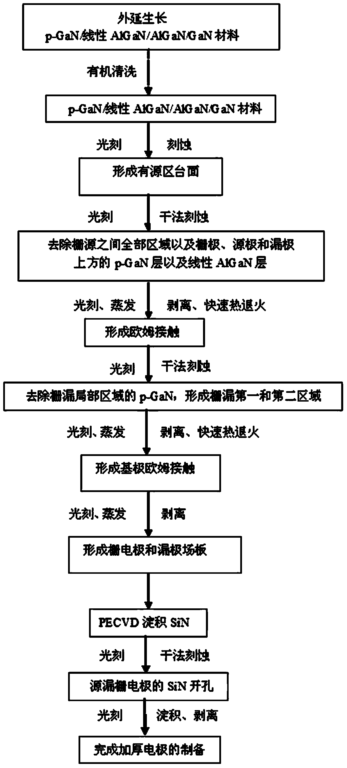
[0040] The present invention will be specifically introduced below in conjunction with the accompanying drawings and specific embodiments.

[0041] Firstly, the structure of the composite drain-based AlGaN / GaN MISHEMT high voltage device of the present invention is introduced.

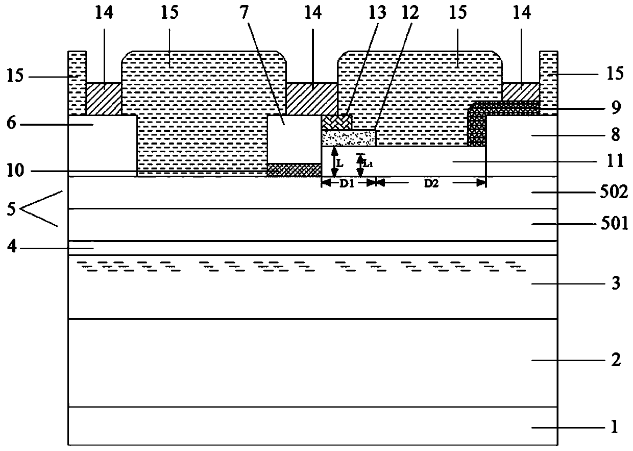
[0042] refer to figure 1 , the AlGaN / GaN MISHEMT high-voltage device based on the composite drain of the present invention, its structure includes from bottom to top: substrate 1, GaN buffer layer 2, intrinsic GaN channel layer 3 (intrinsic GaN channel layer 3 can also be replace with an AlGaN channel layer), an AlN isolation layer 4 and an AlGaN barrier layer 5, and the AlGaN barrier layer 5 is composed of a lower i-type AlGaN layer 501 and an upper n-type AlGaN layer 502, wherein, on the AlGaN barrier layer 5 Along the horizontal direction, there are: source 6, gate 7 and composite drain, and an insulating dielectric layer 10 is also arranged between the gate 7 and the AlGaN barrier layer 5. The ins...


PUM

PropertyMeasurementUnit
thicknessaaaaaaaaaa

Abstract

The invention discloses a composite drain-based AlGaN/GaN MIS-HEMT (Metal-Insulator-Semiconductor High-Electron-Mobility Transistor) high-voltage device and a fabrication method thereof. The structure of the device comprises a substrate, a GaN buffer layer, an intrinsic GaN channel layer, an AlN isolating layer and an AlGaN barrier layer sequentially from the bottom up, a source, a grid and a composite drain are arranged on the AlGaN barrier layer, and an insulating medium layer is arranged between the grid and the AlGaN barrier layer; a linear AlGaN layer, a P-type GaN epitaxial layer and a base are sequentially epitaxially arranged on the top of the AlGaN barrier layer between the grid and the composite drain. The invention has the advantages that: when the device is switched on, the 2DEG (2-dimensional electron gas) concentration of a first region and a second region between the grid and the drain increases, and the resistance decreases; when the device is switched off, the 2DEG of the first region is reduced, the 2DEG of the second region is the same as when the device is switched on, the width of the depletion region of the device is increased, the distribution of an electric field is changed, and the breakdown voltage of the device is increased; the composite grid structure prevents the electric field peak from appearing at the edge of the drain, thus increasing the breakdown voltage of the device; an insulated grid structure prevents grid leakage current, and thereby the performance of the device is enhanced.

Description

technical field [0001] The invention relates to a high-voltage device and a manufacturing method thereof, in particular to a composite drain-based AlGaN / GaN high-voltage, low-on-resistance high-voltage device and a manufacturing method thereof, which can be used to manufacture high-voltage and low-on-resistance AlGaN / GaN MISHEMT high electron mobility transistor belongs to the technical field of microelectronics. Background technique [0002] In recent years, the third-generation wide bandgap semiconductors represented by SiC and GaN have the characteristics of large bandgap, high breakdown electric field, high thermal conductivity, high saturated electron velocity and high concentration of two-dimensional electron gas at the heterojunction interface. Widespread concern. In theory, high electron mobility transistor HEMT, light emitting diode LED, laser diode LD and other devices made of these materials have obvious superior characteristics than existing devices, so in recen...

Claims


Application Information

Patent Timeline
Patent Type & Authority Applications(China)
IPC IPC(8): H01L29/778H01L29/06H01L29/417H01L29/423
CPCH01L29/0634H01L29/0847H01L29/402H01L29/42356H01L29/66462H01L29/7786
Inventor 冯倩杜锴杜鸣张春福梁日泉郝跃
Owner XIDIAN UNIV
Why Eureka
Try Eureka