Supercharge Your Innovation With Domain-Expert AI Agents!

CCD manufacturing technology based on non-intrinsic impurity adsorbing technology

A manufacturing process and extrinsic technology, which is applied in the field of CCD manufacturing process based on extrinsic gettering technology, can solve the problem of reducing the stress of silicon nitride film, disappearing extrinsic gettering effect, and reducing gettering effect in the strain region and other issues, to achieve the effect of improving gettering ability, reducing dark current, and improving device quality

Inactive Publication Date: 2014-05-07
THE 44TH INST OF CHINA ELECTRONICS TECH GROUP CORP
View PDF8 Cites 3 Cited by
  • Summary
  • Abstract
  • Description
  • Claims
  • Application Information

AI Technical Summary

Problems solved by technology

In the prior art, when the gettering treatment is performed on the impurities introduced in the CCD process, an extrinsic gettering region is generally formed in the strained region and the damaged region; although the strained region and the damaged region will not The high temperature conditions in the CCD process completely fail, but the high temperature conditions in the CCD process will still have a negative impact on the strain area and the damaged area: the high temperature conditions in the CCD process will anneal the damaged area, making the damage on the damaged area The number of centers gradually decreases, reducing the gettering effect of the damaged area; the high temperature conditions in the CCD process will also anneal the strained area, reducing the stress of the silicon nitride film or polysilicon film, and reducing the gettering effect of the strained area; Moreover, if the strained region and the damaged region are exposed to high temperature for too long, it may also cause the complete disappearance of the extrinsic gettering effect.

Method used


Image

  • CCD manufacturing technology based on non-intrinsic impurity adsorbing technology

Examples


Embodiment approach

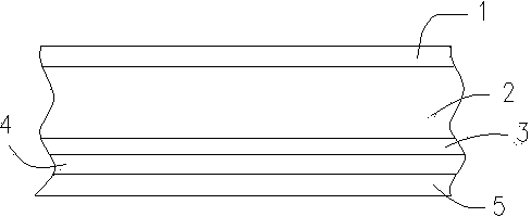
[0026] The silicon substrate is provided as follows:

[0027] A. Deposit a silicon film on the upper surface of the substrate layer 2 by CVD (chemical vapor deposition), and the deposited silicon film forms the epitaxial layer 1. The thickness of the epitaxial layer is usually 8-20 μm, and the doping concentration of boron ions in the epitaxial layer is usually 4E14~2E15cm -3 ;

[0028] B. Treat the lower surface of the substrate layer 2 by means of mechanical damage, laser damage or ion implantation damage to form a damaged layer 3 on the back, and the density of the damage center is 2E14cm -3 above;

[0029] C. Deposit a polysilicon film or a silicon nitride film on the surface of the damaged layer 3 on the back side by CVD, the polysilicon film or silicon nitride film forms the strained layer 4, and the thickness of the strained layer is more than 800nm;

[0030] The gate dielectric is formed, and the gate dielectric is SiO 2 / Si 3 N 4 Composite medium.

[0031] The ...


PUM

PropertyMeasurementUnit
Thicknessaaaaaaaaaa

Abstract

The invention relates to a CCD manufacturing technology based on a non-intrinsic impurity adsorbing technology. The CCD manufacturing technology includes the following step of providing a silicon substrate and is characterized in that the silicon substrate is provided according to the following steps that firstly, a CVD manner is adopted for depositing a silicon thin film on the upper surface of a substrate layer; secondly, a mechanical damaging manner or a laser damaging manner or an ion injection damaging manner is used for processing the lower surface of the substrate layer to form a back damaging layer; thirdly, the CVD manner is adopted for depositing a polycrystalline silicon thin film or a silicon nitride thin film on the surface of the back damaging layer. The CCD manufacturing technology has the advantages that a technological means is used for improving the impurity adsorbing capacity of a non-intrinsic impurity adsorbing layer, the cleanliness of an epitaxial layer is constantly maintained at a good state, dark currents of a finished CCD are reduced and the quality of the device is improved.

Description

technical field [0001] The invention relates to a CCD manufacturing technology, in particular to a CCD manufacturing process based on extrinsic gettering technology. Background technique [0002] The conventional steps of the CCD manufacturing process are: providing a silicon substrate (that is, the substrate layer) → forming a gate dielectric → forming a channel resistance → forming a channel → forming a transfer gate → forming a ground → forming an amplifier source and drain → connecting via holes → forming metal leads ; Among them, what is related to the improvement point of this paper is to provide a silicon substrate; [0003] The epitaxial silicon wafer is a commonly used substrate layer structure. Compared with the CCD manufactured with the single crystal silicon wafer as the substrate layer before, the CCD manufactured with the epitaxial silicon wafer as the substrate layer has lower dark current, especially for working in For CCD under high temperature envi...

Claims


Application Information

Patent Timeline
IPC IPC(8): H01L27/146H01L27/148
Inventor 雷仁方高建威韩沛东廖乃镘李华高
Owner THE 44TH INST OF CHINA ELECTRONICS TECH GROUP CORP
Features
  • R&D
  • Intellectual Property
  • Life Sciences
  • Materials
  • Tech Scout
  • Unparalleled Data Quality
  • Higher Quality Content
  • 60% Fewer Hallucinations
Learn More