Operational amplifiers, level switching circuit and programmable gain amplifier

A technology of operational amplifiers and conversion circuits, which is applied in the direction of improving amplifiers to reduce nonlinear distortion, differential amplifiers, and DC-coupled DC amplifiers. problem, to meet the effect of large output swing and high linearity

Active Publication Date: 2014-05-07
HUAWEI TECH CO LTD
View PDF6 Cites 20 Cited by
  • Summary
  • Abstract
  • Description
  • Claims
  • Application Information

AI Technical Summary

Problems solved by technology

[0009] (1) The conversion function from high level to low level cannot be realized;
[0010] (2) Due to the channel length modulation effect of MOS transistors, with the different voltages at both ends of the drain and source, the same drain current will also lead to different gate-source voltages Vgs
However, when the frequency of the input signal Vin increases, the parasitic capacitance increases due to the increase of the channel length. On the one hand, the maximum input signal frequency is limited, and on the other hand, the increased parasitic capacitance will also deteriorate the linearity of the output signal Vout.
[0011] (3) When the open-loop source follower drives a large capacitive or resistive load, as the input signal changes, the load will draw different currents from the current source Is10, which will change the current flowing through the PMOS transistor M10 Current, so that the gate-source voltage Vgs changes with the input signal, which deteriorates the linearity of the output signal Vout

Method used


Image

  • Operational amplifiers, level switching circuit and programmable gain amplifier
  • Operational amplifiers, level switching circuit and programmable gain amplifier
  • Operational amplifiers, level switching circuit and programmable gain amplifier

Examples


Embodiment Construction

[0042] The technical solutions in the embodiments of the present invention will be clearly and completely described below in conjunction with the accompanying drawings in the embodiments of the present invention. Obviously, the described embodiments are only a part of the embodiments of the present invention, rather than all the embodiments. Based on the embodiments of the present invention, all other embodiments obtained by those of ordinary skill in the art without creative work shall fall within the protection scope of the present invention.

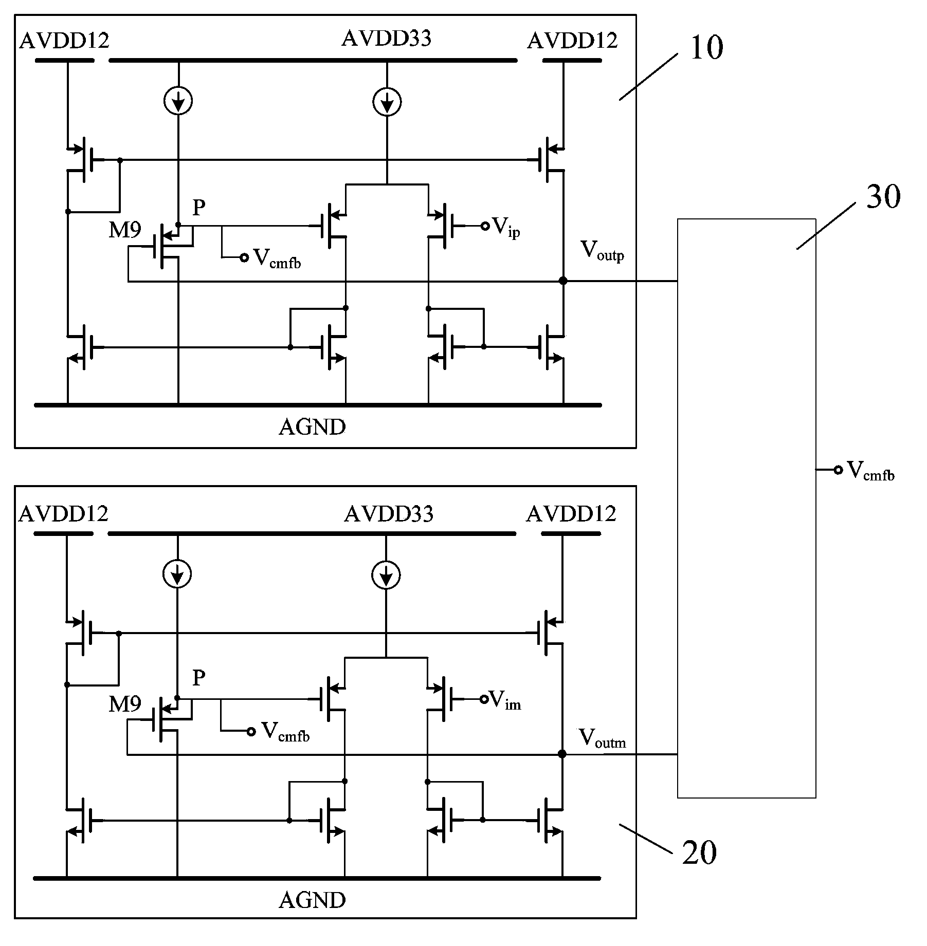
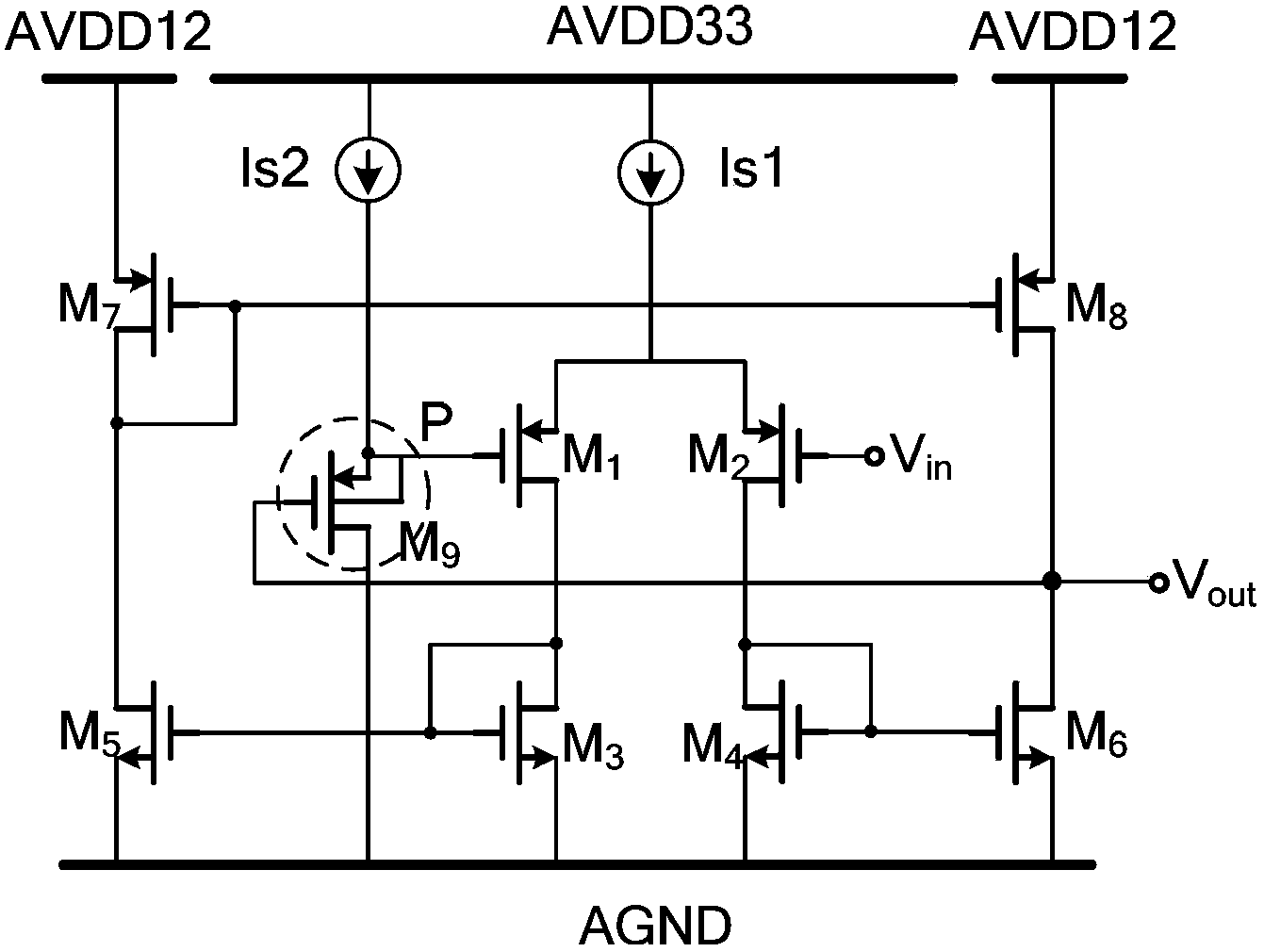
[0043] An operational amplifier, a level conversion circuit, and a programmable gain amplifier are provided in the embodiment of the present invention, which can realize the functions of converting from low level to high level and from high level to low level at the same time, and can satisfy Output large swing and high linearity requirements.

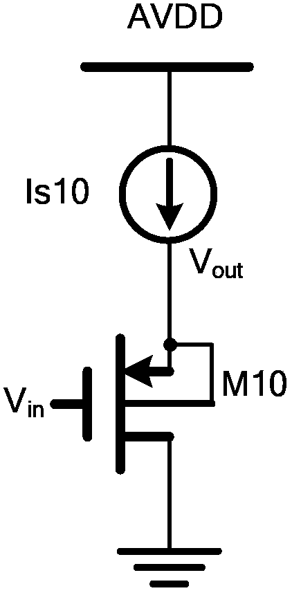
[0044] Reference figure 2 , Is a circuit diagram of an operational amplifier provided by an em...


PUM


Abstract

The embodiment of the invention discloses a level switching circuit which comprises two operational amplifiers and a common-mode feedback loop. A substrate and a PMOS source follower which is connected with a source electrode are inserted in a P point of each operational amplifier, so that big difference oscillation amplitude 3.3V high common-mode level is horizontally moved to 1.2V low common mode level with low degree of distortion, and the difference oscillation amplitude is kept unchanged. The common-mode feedback loop receives output signals of the two operational amplifiers, common-mode taking operation is conducted on the two output signals, an obtained common-mode value is compared to a set reference voltage, and the comparison result is used as a feedback signal to be output to the two operational amplifiers. The embodiment of the invention further provides the operational amplifiers and a programmable gain amplifier. According to the level switching circuit, the operational amplifiers and the programmable gain amplifier, the function of switching from low level to high level and the function of switching from the high level to the low level can be achieved at the same time, and the demand for large outputting oscillation amplitude and high linearity is met.

Description

Technical field [0001] The present invention relates to the field of semiconductor technology, in particular to an operational amplifier, a level conversion circuit and a programmable gain amplifier. Background technique [0002] In the analog-digital hybrid chip, it is often necessary to shift the level of the continuous analog signal at the analog front end, while ensuring the quality of the transferred signal (such as swing amplitude, linearity, etc.). Generally, considering performance, voltage margin and other reasons, analog front-end circuits are often designed with IO devices that work in the high-voltage domain. Taking into account the power consumption area and other reasons, digital and analog-to-digital converters are implemented using core devices that work in the low-voltage domain. Therefore, the level conversion circuit needs to move the analog signal from the high-voltage domain to the low-voltage domain, which involves not only the conversion of the voltage dom...

Claims


Application Information

Patent Timeline
Patent Type & Authority Applications(China)
IPC IPC(8): H03F3/45H03F1/32H03G3/30H03K19/0185
Inventor 杨金达周立人熊俊林敬新
Owner HUAWEI TECH CO LTD
Why Eureka
Try Eureka