Low-range and high-sensitivity micro-electromechanical system (MEMS) pressure sensor and manufacture method thereof

A pressure sensor, high-sensitivity technology, applied in the direction of measuring force, fluid pressure measurement by changing the ohmic resistance, instruments, etc., can solve the practical requirements of carbon nanotubes and device preparation processes that are difficult to be compatible, large-area and batch preparation There are problems such as distance, achieving considerable economic and social benefits, improving sensitivity, and ensuring the linearity of devices

Inactive Publication Date: 2014-03-19
INST OF SEMICONDUCTORS - CHINESE ACAD OF SCI
View PDF5 Cites 10 Cited by
  • Summary
  • Abstract
  • Description
  • Claims
  • Application Information

AI Technical Summary

Problems solved by technology

For example, based on the research on the piezoresistive properties of single-walled and multi-walled carbon nanotubes, carbon nanotube low-pressure sensors are applied to touch screens or flexible displays. The compatibility of carbon nanotubes and device preparation processes is a difficult point, and the distance There is still a distance between the practical requirements of area and batch preparation

Method used


Image

  • Low-range and high-sensitivity micro-electromechanical system (MEMS) pressure sensor and manufacture method thereof
  • Low-range and high-sensitivity micro-electromechanical system (MEMS) pressure sensor and manufacture method thereof
  • Low-range and high-sensitivity micro-electromechanical system (MEMS) pressure sensor and manufacture method thereof

Examples


Embodiment

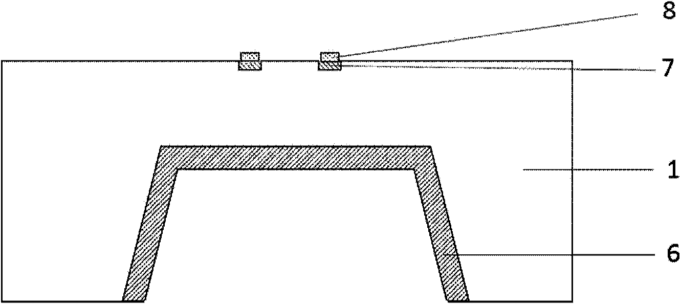
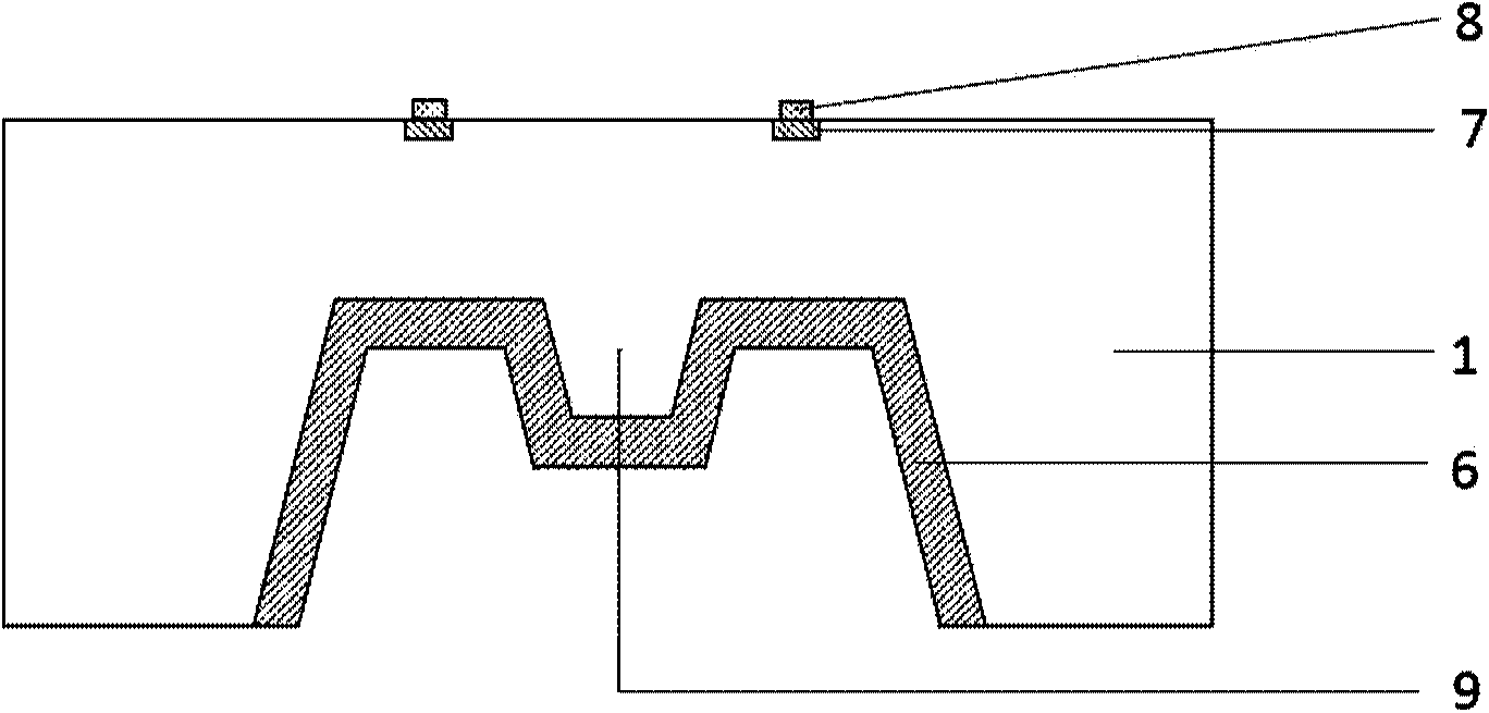
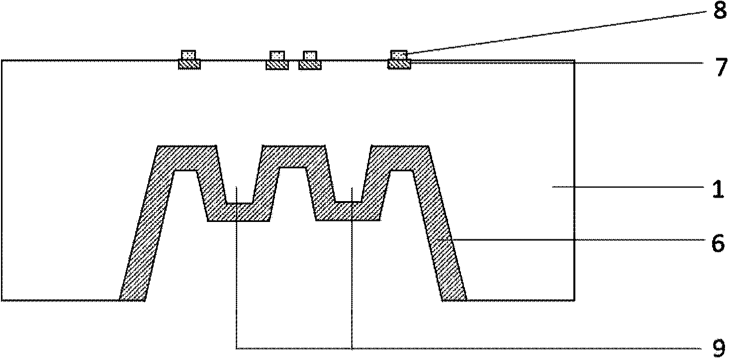
[0044] Such as figure 1 An example of a structure, incorporating as Figure 4-1 to Figure 4-9 Described technological process, specifically as follows:

[0045] (1) if Pic 4-1 As shown, a double-thrown silicon substrate 1 is selected and subjected to high-temperature oxidation to form a silicon oxide layer 2 on both sides of the silicon substrate.

[0046] (2) if Figure 4-2 As shown, the low-pressure chemical vapor deposition (LPCVD) method is used to deposit the silicon nitride film 3 on the front and back sides of the above-mentioned silicon substrate 1 with the oxide layer 2, and the ratio of the Si source and the N source during the reaction is reasonably adjusted to realize Low stress and corrosion resistant silicon nitride (SiNx) layer.

[0047] (3) if Figure 4-3 As shown, the mask window is defined by photolithography on the back of the silicon wafer, and the silicon nitride film 3 and silicon oxide layer 2 in the window area are etched away by dry etching techn...


PUM

PropertyMeasurementUnit
thicknessaaaaaaaaaa

Abstract

The invention discloses a low-range and high-sensitivity micro-electromechanical system (MEMS) pressure sensor which comprises a monocrystalline silicon layer (1), a porous silicon / silicon composite membrane structure (6), a porous silicon voltage dependent resistor (7) and a metal layer (8), wherein the back surface of the monocrystalline silicon layer (1) is provided with a concave cavity; the porous silicon / silicon composite membrane structure (6) is formed in the concave cavity in the back surface of the monocrystalline silicon layer (1); the porous silicon voltage dependent resistor (7) is formed on the front surface of the monocrystalline silicon layer (1); the metal layer (8) is deposited on the porous silicon voltage dependent resistor (7) and has a function of metal interconnection. The invention further discloses a manufacture method of the low-range and high-sensitivity MEMS pressure sensor. Porous silicon materials have excellent piezoresistive performance and mechanical performance, and therefore, the porous silicon MEMS pressure sensor adopting the structure can keep degree of linearity and improve sensitivity simultaneously, and can be applied within a superlow pressure range by means of flexible structure design.

Description

technical field [0001] The invention belongs to the technical field of MEMS pressure sensor manufacturing, and in particular relates to a low-range high-sensitivity MEMS pressure sensor based on a double-sided porous silicon material and a manufacturing method thereof. Background technique [0002] MEMS pressure sensors overcome the defects of traditional mechanical pressure sensors, and have the outstanding advantages of miniaturization, high sensitivity, good stability, low cost, easy integration and intelligence. Sensitivity and nonlinearity are the most important technical parameters of pressure sensors. Its sensitive mechanism is based on the mechanical deformation and stress of the pressure-sensitive film caused by the measured pressure. Typical forms include piezoresistive, capacitive and resonant. Compared with capacitive and resonant pressure sensors, the manufacturing process and signal processing circuit of piezoresistive pressure sensors are simple, and there is...

Claims


Application Information

Patent Timeline
Patent Type & Authority Applications(China)
IPC IPC(8): G01L9/02G01L1/20B81C1/00
Inventor 赵永梅季安张明亮杨香宁瑾王晓东杨富华
Owner INST OF SEMICONDUCTORS - CHINESE ACAD OF SCI
Why Eureka
Try Eureka