
Thin-film organic photodetector with pin structure and its preparation method and application

A detector and structured light technology, applied in semiconductor/solid-state device manufacturing, photovoltaic power generation, electric solid-state devices, etc., can solve the problem of low performance of thin-film photoconductive detectors, achieve high photocurrent and photoelectric performance, simple preparation method, The effect of improving responsiveness

Active Publication Date: 2017-04-12
INST OF CHEM CHINESE ACAD OF SCI
View PDF3 Cites 0 Cited by
  • Summary
  • Abstract
  • Description
  • Claims
  • Application Information

AI Technical Summary

Problems solved by technology

[0018] In order to overcome the shortcomings of low performance of existing thin film photoconductive detectors, the present invention provides a thin film organic photoconductive detector with simple structure, convenient preparation method and very high photoelectric performance

Method used


Image

  • Thin-film organic photodetector with pin structure and its preparation method and application
  • Thin-film organic photodetector with pin structure and its preparation method and application
  • Thin-film organic photodetector with pin structure and its preparation method and application

Examples


Embodiment 1

[0071] 1) The substrate 4 is pretreated as follows: the substrate 4 is washed with deionized water, acetone and isopropanol successively, and then dried.

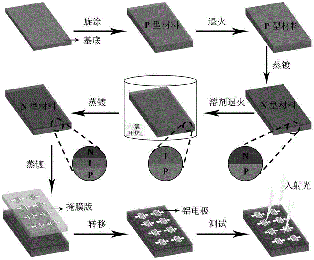
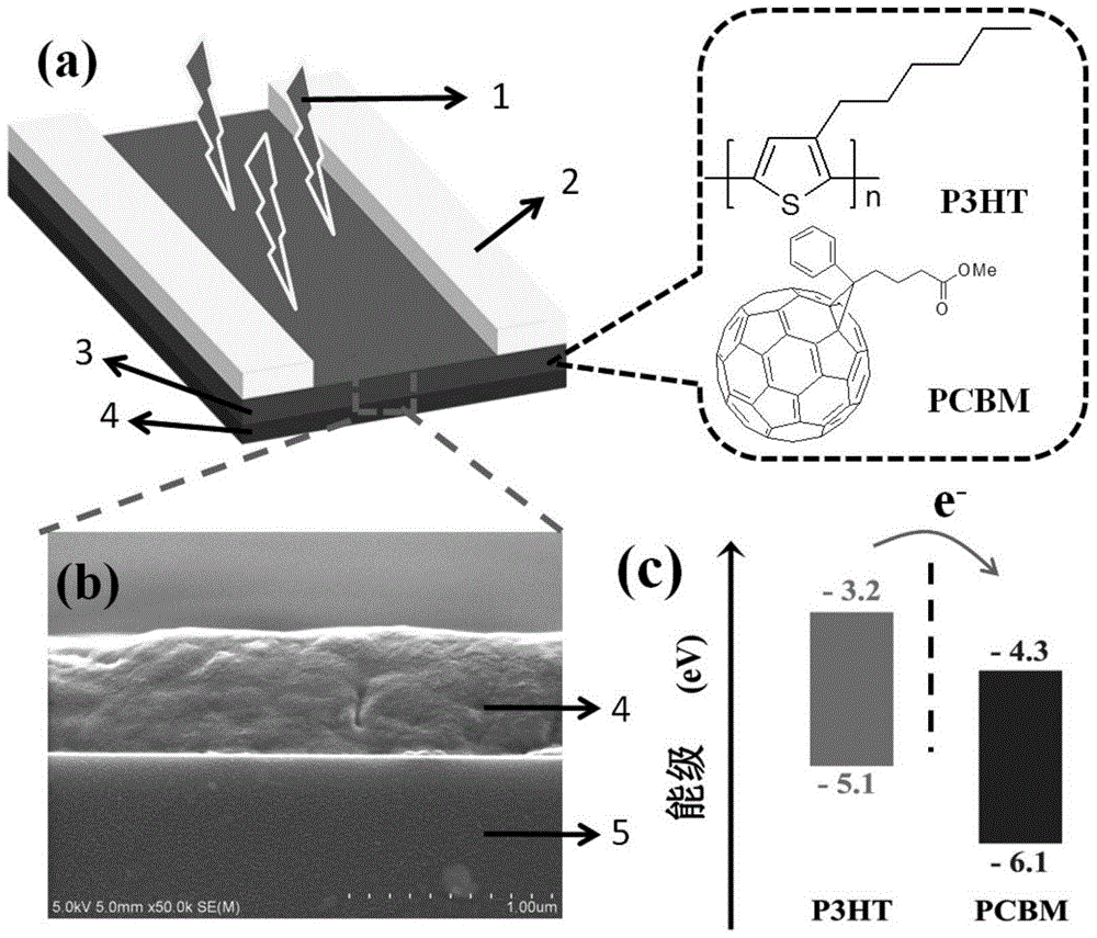
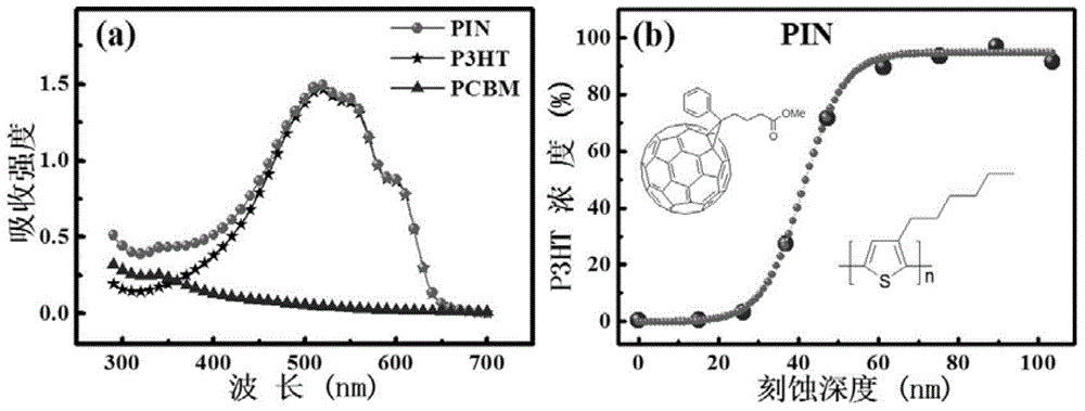
[0072] 2) if figure 1 , preparing PIN organic material layer 3 on substrate 4, the specific steps include: dissolving P3HT with a relative molecular weight of 40000g / mol in o-dichlorobenzene to obtain a solution with a concentration of 40mg / ml, and annealing the substrate after spin coating at 1000rpm for 60s 100°C for 10 minutes to obtain a P-layer organic layer with a thickness of 500nm, and then vapor-deposit a 20nm-thick N layer (PCBM layer with a relative molecular mass of 910.88g / mol) on it and put it into an atmosphere filled with dichloromethane in an airtight container for 1 min. Because dichloromethane can dissolve PCBM very well and dissolve P3HT in a small amount, PCBM will absorb dichloromethane and slowly diffuse into the P3HT layer to form an I layer (mixed heterojunction layer P3HT:PCBM), when on it A 20 n...


PUM


Abstract

The invention discloses a thin-film organic photodetector based on a PIN structure, a preparation method and an application thereof. The thin-film organic photoconductive detector includes a substrate, a photosensitive layer with a PIN structure and a patterned electrode layer thereon. The detector combines the high mobility of the intrinsic organic layers (P and N layers) with the high concentration of photofree charges generated by the organic heterojunction layer (I layer, which is a mixture of P and N organic materials). The advantages. The high mobility results in short electron transit times, and the generation of high-concentration photofree charges imply high external quantum efficiency. Therefore, when light is irradiated on the device, the material absorbs light and generates carriers quickly, and a large number of them are collected by the electrodes to generate high photocurrent and photoelectric performance, thereby improving the sensitivity of the detector. Therefore, this thin-film organic photodetector has important application value.

Description

technical field [0001] The invention relates to a novel thin-film organic photodetector with PIN structure, its preparation method and application. Background technique [0002] At present, the known photoconductive detector structure is composed of two horizontal electrodes and a photosensitive layer in the middle. Connect the photoconductive device into a loop and add a bias electric field. When the incident light contacts the detector, the photosensitive layer inside the detector generates electron-hole pairs, which are separated under the action of the electric field and collected by the electrodes. Photocurrent is formed, and the intensity and size of light can be characterized by the intensity of photocurrent, which can be used for light detection, image imaging or biosensing and other directions. Therefore, the sensitivity of the device to light is very important, and two important parameters are usually used to characterize such a sensitivity: responsivity R and pho...

Claims


Application Information

Patent Timeline
Patent Type & Authority Patents(China)
IPC IPC(8): H01L51/42H01L51/44H01L51/48
CPCH10K30/40H10K30/20Y02E10/549
Inventor 靳志文王吉政
Owner INST OF CHEM CHINESE ACAD OF SCI
Learn More