A method for improving heat dissipation efficiency of semiconductor laser chip
A chip heat dissipation and laser technology, applied in the laser field, can solve the problems of poor heat dissipation efficiency, achieve the effects of reducing production costs, reducing thermal resistance, and improving optical power output
- Summary
- Abstract
- Description
- Claims
- Application Information
AI Technical Summary
Problems solved by technology
Method used
Image
Examples
Embodiment 1
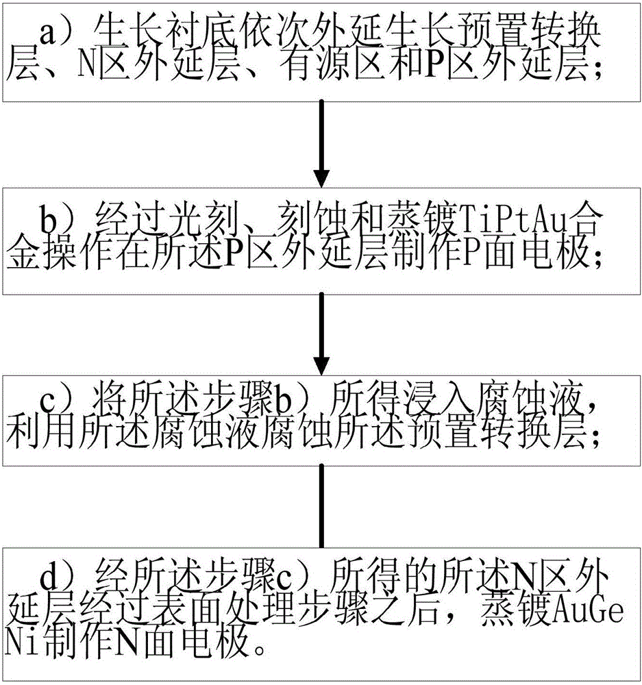
[0027] Such as Figure 1-5 Shown, a kind of manufacturing method of semiconductor laser chip of the present invention comprises the following steps:
[0028] a) Growth substrate 1 epitaxially grows preset conversion layer 5 , N-region epitaxial layer 2 , active region 3 and P-region epitaxial layer 4 in sequence;
[0029] b) Fabricate the P-side electrode 6 on the P-region epitaxial layer 4 through photolithography, etching, evaporation of TiPtAu and annealing;
[0030] c) immersing the obtained product in step b) into the corrosion solution, and using the corrosion solution to corrode the preset conversion layer 5;
[0031] d) After the surface treatment step of the N-region epitaxial layer 2 obtained in step c), AuGeNi is evaporated to prepare the N-face electrode 8 .
[0032] The P-face electrode 6 and the N-face electrode 8 respectively form a P-face heat dissipation structure 7 and an N-face heat dissipation structure 9 .
[0033] The P-region epitaxial layer 4 include...
Embodiment 2
[0039] Such as Figure 1-5 Shown, a kind of manufacturing method of semiconductor laser chip of the present invention comprises the following steps:
[0040] a) Growth substrate 1 epitaxially grows preset conversion layer 5 , N-region epitaxial layer 2 , active region 3 and P-region epitaxial layer 4 in sequence;
[0041] b) Fabricate the P-side electrode 6 on the P-region epitaxial layer 4 through photolithography, etching, evaporation of TiPtAu and annealing;
[0042] c) immersing the obtained product in step b) into the corrosion solution, and using the corrosion solution to corrode the preset conversion layer 5;
[0043] d) After the surface treatment step of the N-region epitaxial layer 2 obtained in step c), AuGeNi is evaporated to prepare the N-face electrode 8 .
[0044] The P-face electrode 6 and the N-face electrode 8 respectively form a P-face heat dissipation structure 7 and an N-face heat dissipation structure 9 .
[0045] The N-surface heat dissipation structu...
Embodiment 3
[0053] Such as Figure 1-5 Shown, a kind of manufacturing method of semiconductor laser chip of the present invention comprises the following steps:
[0054] a) Growth substrate 1 epitaxially grows preset conversion layer 5 , N-region epitaxial layer 2 , active region 3 and P-region epitaxial layer 4 in sequence;
[0055] b) Fabricate the P-side electrode 6 on the P-region epitaxial layer 4 through photolithography, etching, evaporation of TiPtAu and annealing;
[0056] c) immersing the obtained product in step b) into the corrosion solution, and using the corrosion solution to corrode the preset conversion layer 5;
[0057] d) After the surface treatment step of the N-region epitaxial layer 2 obtained in step c), AuGeNi is evaporated to prepare the N-face electrode 8 .
[0058] The P-face electrode 6 and the N-face electrode 8 respectively form a P-face heat dissipation structure 7 and an N-face heat dissipation structure 9 .
[0059] The N-surface heat dissipation structu...
PUM
 Abstract
Description
Claims
Application Information
 - R&D
- Intellectual Property
- Life Sciences
- Materials
- Tech Scout
- Unparalleled Data Quality
- Higher Quality Content
- 60% Fewer Hallucinations
Browse by: Latest US Patents, China's latest patents, Technical Efficacy Thesaurus, Application Domain, Technology Topic, Popular Technical Reports.
© 2025 PatSnap. All rights reserved.Legal|Privacy policy|Modern Slavery Act Transparency Statement|Sitemap|About US| Contact US: help@patsnap.com


