Method for contactlessly breaking polycrystalline silicon

A polysilicon, non-contact technology, applied in the direction of grain processing, etc., can solve the problems of increasing steps, low overall efficiency of crushing, and increasing the risk of polysilicon rod contamination, so as to achieve the effect of improving efficiency and reducing the risk of pollution

Inactive Publication Date: 2014-05-28
ASIA SILICON QINGHAI
View PDF7 Cites 11 Cited by
  • Summary
  • Abstract
  • Description
  • Claims
  • Application Information

AI Technical Summary

Problems solved by technology

Although this method also avoids the disadvantage of low efficiency of manual crushing, this method not only has an extra step of moving polysilicon rods than manual crushing, but also increases the step of drying the crushed polysilicon rods, so the overall efficiency of this method may be broken. Less efficient than manual crushing
Not only that, but during the whole crushing process of this method, the polysilicon rods are in contact with water and drying medium, which increases the risk of polysilicon rods being polluted

Method used


Image

  • Method for contactlessly breaking polycrystalline silicon
  • Method for contactlessly breaking polycrystalline silicon
  • Method for contactlessly breaking polycrystalline silicon

Examples


Embodiment 1

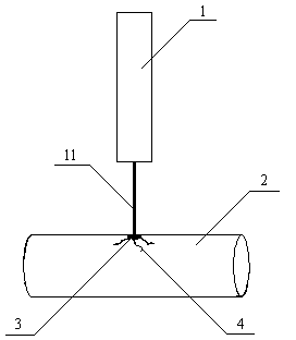
[0035] Such as figure 1 As shown, the method for non-contact laser crushing of polycrystalline silicon rods or polycrystalline silicon blocks of the present invention can be described in more detail. A laser beam 11 is generated by a laser 1 . When the laser beam 11 irradiates the local area 3 of the polycrystalline silicon rod or polycrystalline silicon block 2 , the energy of the laser beam 11 is absorbed by the local area 3 of the polycrystalline silicon rod or polycrystalline silicon block 2 . After the local region 3 of the polycrystalline silicon rod or polycrystalline silicon block 2 absorbs the energy of the laser beam 11, the temperature of the local region 3 of the polycrystalline silicon rod or polycrystalline silicon block 2 rises rapidly. As the temperature of the local region 3 of the polycrystalline silicon rod or polycrystalline silicon block 2 increases, the density of the local region 3 of the polycrystalline silicon rod or polycrystalline silicon block 2 de...

Embodiment 2

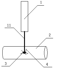
[0040] Lasers 1 with longer wavelengths can also be used when carrying out the method of the invention for non-contact fragmentation of polycrystalline silicon rods or polycrystalline silicon blocks by laser. exist figure 2 In the embodiment, the laser beam is an infrared laser beam 11, that is, a laser beam with a wavelength of 1064 nanometers. When using an infrared laser, since the polycrystalline silicon rod or polycrystalline silicon block 2 has a small absorption coefficient for infrared light, the focus of the laser beam must be adjusted to the internal point of the polycrystalline silicon rod or polycrystalline silicon block 2, that is, the local area 3 . After the point of the polycrystalline silicon rod or the polycrystalline silicon block 2, that is, the local area 3, is irradiated by the infrared laser beam 11, the temperature of the point of the polycrystalline silicon rod or the polycrystalline silicon block 2, that is, the local area 3, rises rapidly, and a hug...

Embodiment 3

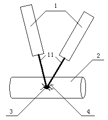
[0042] In other applications of the method for non-contact breaking of polycrystalline silicon rods or polycrystalline silicon blocks by laser of the present invention, multiple lasers can be used to achieve the purpose of breaking polycrystalline silicon rods or polycrystalline silicon blocks 2 . image 3 An embodiment of the invention using 2 lasers 1 for fragmenting polysilicon rods or blocks 2 is shown. In this embodiment, two infrared lasers 1 each generate an infrared laser beam 11 . Both infrared laser beams 11 are focused on a point, ie a local area 3 , of the polysilicon rod or block 2 . After the point of the polycrystalline silicon rod or the polycrystalline silicon block 2, that is, the local area 3, is irradiated by two infrared laser beams 11, the temperature of the point of the polycrystalline silicon rod or the polycrystalline silicon block 2, that is, the local area 3, rises rapidly. A huge temperature gradient is formed, and this huge temperature gradient cr...


PUM

PropertyMeasurementUnit
diameteraaaaaaaaaa
wavelengthaaaaaaaaaa

Abstract

The invention discloses a method for contactlessly breaking polycrystalline silicon, and more specifically discloses a method for breaking polycrystalline silicon by using laser technology. According to the method for contactlessly breaking polycrystalline silicon, at least one laser beam is irradiated to a polycrystalline silicon rod or polycrystalline silicon ingot; and once local area on the surface of or in the polycrystalline silicon rod or polycrystalline silicon ingot absorbs laser energy, the local area of the polycrystalline silicon rod or polycrystalline silicon ingot is heated instantaneously. The heated local area of the polycrystalline silicon rod or polycrystalline silicon ingot expands; and thermal expansion stress is generated on the surface of or in the polycrystalline silicon rod or polycrystalline silicon ingot, so that the polycrystalline silicon rod or polycrystalline silicon ingot is broken.

Description

technical field [0001] The invention relates to a production method of polysilicon, in particular to a method for crushing polysilicon in the production process of polysilicon. Background technique [0002] At present, polysilicon, the raw material of most crystalline silicon in the world, is produced by the improved Siemens method. The so-called improved Siemens method to produce polysilicon is to reduce high-purity trichlorosilane with high-purity hydrogen at high temperature, and the polysilicon produced is deposited on the silicon core. As polysilicon is continuously deposited on the silicon core, the diameter of the silicon core gradually increases, and finally a polysilicon rod is formed. The diameter of polycrystalline silicon rods is generally between 15 and 30 cm. [0003] The polycrystalline silicon rods produced by the improved Siemens method are the raw materials for monocrystalline silicon columns and polycrystalline silicon ingots required by the semico...

Claims


Application Information

Patent Timeline
Patent Type & Authority Applications(China)
IPC IPC(8): B02C19/18
Inventor 季静佳王体虎
Owner ASIA SILICON QINGHAI
Why Eureka
Try Eureka