
A Pretreatment Process for Improving the Quality of Polysilicon Thin Film

A technology of polycrystalline silicon thin film and amorphous silicon thin film, which is applied in the direction of polycrystalline material growth, metal material coating process, crystal growth, etc., can solve the problems of high cost, complicated equipment, unfavorable induced crystallization, etc. Smooth full, large grain size effect

Active Publication Date: 2016-04-06
ZHONGWEI NEW ENERGY CHENGDU CO LTD
View PDF2 Cites 0 Cited by
  • Summary
  • Abstract
  • Description
  • Claims
  • Application Information

AI Technical Summary

Problems solved by technology

[0005] ③The laser crystallization method is fast, but the equipment is complicated and the cost is high; the representative literature report has "C.T.Angelis, C.A.Dimitriadis, F.V.Farmakis, et al., Solid-StateElec., 44 (6) (2000) 1081- 1087."
[0006] ④Metal-induced crystallization method, for Ni, Cu, Pt and other metals used for metal-induced crystallization of amorphous silicon thin films, it is easy to generate deep energy levels in Si and form recombination centers, which will affect the electrical properties of polycrystalline silicon thin film batteries; And these metals are easy to form silicide with Si, which is not conducive to the smooth progress of induced crystallization

Method used


Image

  • A Pretreatment Process for Improving the Quality of Polysilicon Thin Film
  • A Pretreatment Process for Improving the Quality of Polysilicon Thin Film
  • A Pretreatment Process for Improving the Quality of Polysilicon Thin Film

Examples


Embodiment 1

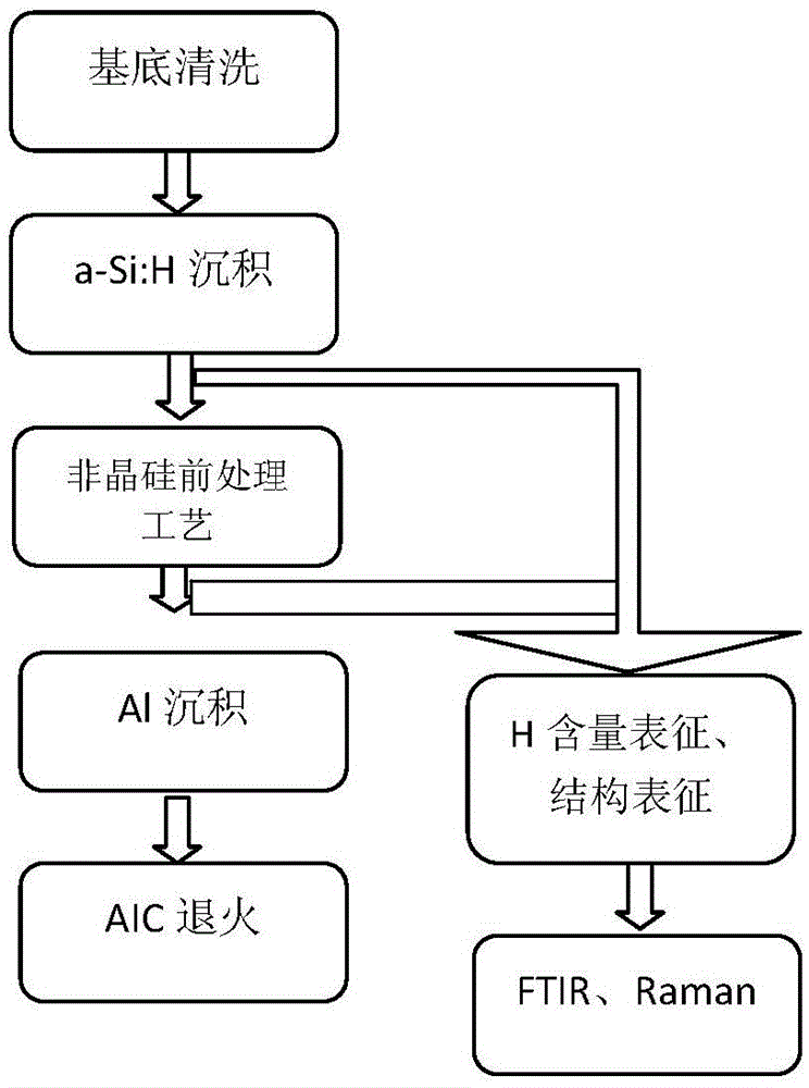
[0024] Embodiment 1 The schematic diagram of the AIC method described in the present invention is as figure 1 shown

[0025] A layer of amorphous silicon (a-Si) is first deposited on the substrate by PECVD. The substrate may be one of a glass substrate, a ceramic substrate, a stainless steel substrate, and the like. The thickness of α-Si:H is between 1nm-1μm. Then vapor-deposit a layer of aluminum (Al) on the amorphous silicon by vacuum coating method, the thickness of aluminum is also between 1nm-1μm, the thickness ratio of α-Si:H and Al is about 1:1, if it cannot be guaranteed, Then the thickness of α-Si:H should be greater than that of Al. After forming the substrate / amorphous silicon / aluminum structure, annealing is performed at a temperature lower than the eutectic temperature of Si and Al at 577°C (it can be as low as about 350°C) to form a substrate / aluminum / polysilicon structure, thereby preparing polysilicon seed layer.

[0026] Utilize the method provided by the...


PUM

PropertyMeasurementUnit
thicknessaaaaaaaaaa

Abstract

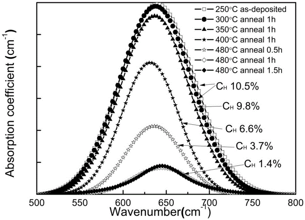
The invention relates to a pretreatment technology for improving the quality of a polycrystalline silicon film. The pretreatment technology is characterized in that the content of hydrogen in noncrystalline silicon is controlled effectively by controlling the annealing temperature and the annealing time before aluminum-induced crystallization (AIC), and the noncrystalline silicon film is annealed in nitrogen or argon shield gas. The annealing temperature is 350-500 DEG C and the annealing time is 0.1-5h. After the noncrystalline silicon film is subjected to annealing treatment at different temperature, the content of hydrogen in the film is reduced to 1.4% from 10%, so that the polycrystalline silicon film prepared via aluminum induction is dry, smooth and complete in surface. According to the pretreatment technology, the high-quality polycrystalline silicon film can be prepared at lower temperature and in shorter time. Compared with the traditional AIC polycrystalline silicon preparation method, an annealing and dehydrogenation step is added before the AIC, so that the content of hydrogen in a precursor a-Si:H can be controlled effectively, and the polycrystalline silicon film with larger grain size, smaller stress and smoother and more complete surface can be prepared.

Description

technical field [0001] The invention relates to a method for preparing a polysilicon film, more specifically to a pretreatment process for inducing crystallization of amorphous silicon by using aluminum to improve the quality of the polysilicon film, and belongs to the field of polysilicon film preparation. Background technique [0002] Polycrystalline silicon (Poly-Si) thin film has high carrier mobility, light absorption rate and stable photoelectric performance, so it is widely used in solar cells, thin film transistors, liquid crystal displays and image sensors. At present, the methods for preparing polysilicon thin films mainly include chemical vapor deposition, solid phase crystallization, laser crystallization and metal-induced crystallization. [0003] Among them, ① chemical vapor deposition method requires high temperature to obtain polysilicon film, and the obtained polysilicon grain size is very small, only nm level; representative literature reports include "Liu ...

Claims


Application Information

Patent Timeline
Patent Type & Authority Patents(China)
IPC IPC(8): C23C14/58C23C28/00C23C16/24C30B29/06
Inventor 端伟元邱羽俞健卞剑涛刘正新
Owner ZHONGWEI NEW ENERGY CHENGDU CO LTD
Learn More