

Method for epitaxial growth of II-type GaSb/InGaAs quantum point on InP substrate
A growth method and technology of quantum dots, applied in the direction of single crystal growth, crystal growth, single crystal growth, etc., can solve the problems of different, quantum dot difficulties, different mobility, etc., and achieve the critical transition thickness reduction, good morphology and quality, Enhanced topographic and optical quality effects
- Summary
- Abstract
- Description
- Claims
- Application Information
AI Technical Summary
Problems solved by technology
Method used
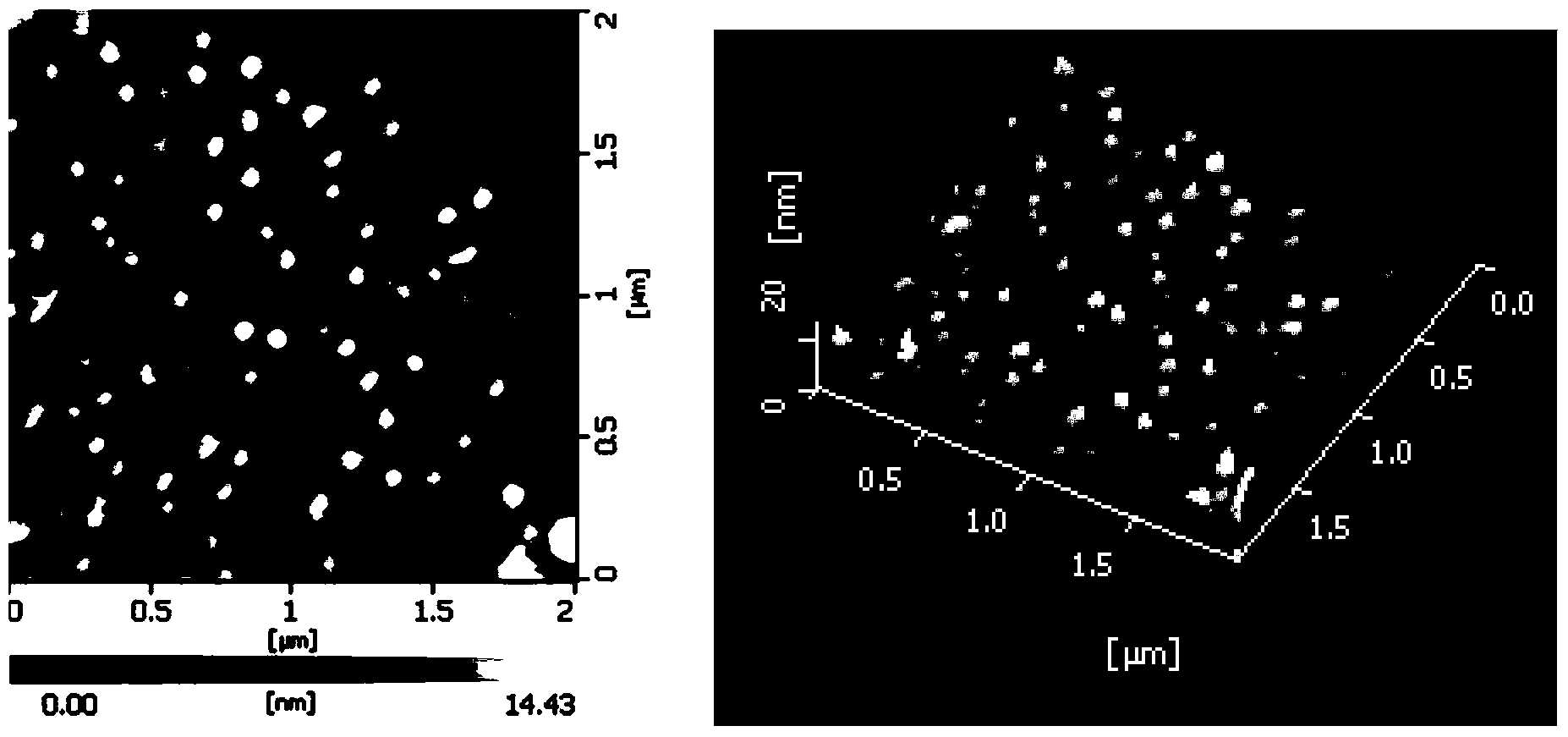
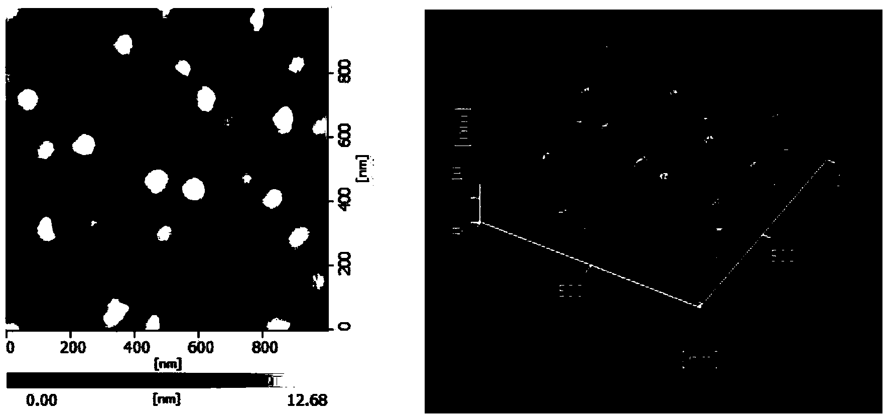
Image

Examples
Embodiment 1
[0045] 1) Remove the surface of the InP substrate from the mold, and clean the surface of the substrate to remove carbon and oxygen, so as to facilitate the growth of In that matches the lattice of the InP substrate. 0.53 Ga 0.47 As buffer layer, the demolding process is carried out under the protection of the As source, the temperature of the substrate thermocouple is 720°C, and the temperature of the As source is 365°C (the temperature of all subsequent As sources is 365°C);
[0046] 2) Growth of superlattice-matched In on the substrate surface 0.53 Ga 0.47 As buffer layer:
[0047] Quickly lower the thermocouple temperature of the substrate to 670°C, open the Ga source and In source shutter, and grow 3000? 0.53 Ga 0.47 The As superlattice-matched buffer layer makes the surface of the InP substrate after demolding smooth and is conducive to the growth of subsequent quantum dots. At this time, the growth temperature of the Ga source is 835°C, the rate is 2350? / h, and the ...
Embodiment 2
[0056] 1) Remove the surface of the InP substrate from the mold, and clean the surface of the substrate to remove carbon and oxygen, so as to facilitate the growth of In that matches the lattice of the InP substrate. 0.53 Ga 0.47 As buffer layer, the demoulding process is carried out under the protection of the As source, the temperature of the thermocouple is 710°C, and the temperature of the As source is 365°C (the temperature of all subsequent As sources is 365°C);
[0057] 2) Growth of superlattice-matched In on the substrate surface 0.53 Ga 0.47 As buffer layer:
[0058] Quickly lower the thermocouple temperature of the substrate to 660°C, open the Ga source and In source shutter, and grow 5000? 0.53 Ga 0.47 The As superlattice-matched buffer layer makes the surface of the InP substrate after demolding smooth and is conducive to the growth of subsequent quantum dots. At this time, the growth temperature of the Ga source is 835°C, the rate is 2350? / h, and the growth ra...
Embodiment 3
[0067] 1) Remove the surface of the InP substrate from the mold, and clean the surface of the substrate to remove carbon and oxygen, so as to facilitate the growth of In that matches the lattice of the InP substrate. 0.53 Ga 0.47As buffer layer, the demoulding process is carried out under the protection of the As source, the temperature of the thermocouple is 715°C, and the temperature of the As source is 365°C (the temperature of all subsequent As sources is 365°C);
[0068] 2) Growth of superlattice-matched In on the substrate surface 0.53 Ga 0.47 As buffer layer:
[0069] Quickly lower the thermocouple temperature of the substrate to 665°C, open the Ga source and In source shutter, and grow 4000? 0.53 Ga 0.47 The As superlattice-matched buffer layer makes the surface of the InP substrate after demoulding flat and is conducive to the growth of subsequent quantum dots. At this time, the growth temperature of the Ga source is 835°C, the rate is 2350? / h, and the growth rate...
PUM
| Property | Measurement | Unit |
|---|---|---|
| size | aaaaa | aaaaa |
Abstract
Description
Claims
Application Information