Epitaxial growth method for improving reverse electric leakage of GaN-based light-emitting diode (LED)

An epitaxial growth and reverse leakage technology, applied in the direction of crystal growth, single crystal growth, single crystal growth, etc., can solve the problems of increasing the forward voltage of the device, deteriorating the device performance, reducing the quantum efficiency of the device, etc., to improve the brightness, reduce the Leakage channel, improve the effect of reverse leakage

Inactive Publication Date: 2014-05-28
合肥彩虹蓝光科技有限公司
View PDF5 Cites 12 Cited by
  • Summary
  • Abstract
  • Description
  • Claims
  • Application Information

AI Technical Summary

Problems solved by technology

These a large number of threading dislocations and V-type defects have become the main leakage channels of LED chips. Holes and electrons will form non-radiative coincidences through threading dislocation lines and V-type defects, reducing the internal quantum efficiency of the device and deteriorating the device. performance
Research [Y.Chen, atl, Applied Physics Letters72,710] shows that the epitaxial AlGaN layer on GaN can significantly suppress the linear defect and V-type defect density in the GaN epitaxial layer, but generally the AlGaN layer insertion will increase the forward direction of the device. Voltage

Method used


Image

  • Epitaxial growth method for improving reverse electric leakage of GaN-based light-emitting diode (LED)
  • Epitaxial growth method for improving reverse electric leakage of GaN-based light-emitting diode (LED)
  • Epitaxial growth method for improving reverse electric leakage of GaN-based light-emitting diode (LED)

Examples


Embodiment 1

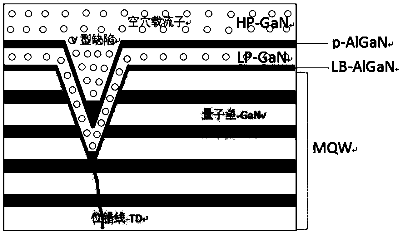
[0026] An epitaxial growth method for improving the reverse leakage of GaN-based LEDs. The LED epitaxial structure includes, from bottom to top, a sapphire substrate, a low-temperature nucleation layer, a high-temperature GaN buffer layer, a high-temperature non-doped GaN layer, and a non-doped GaN layer. AlGaN insertion layer, high temperature non-doped GaN layer, high temperature n-type GaN layer, n-type doped AlGaN layer, high temperature n-type GaN layer, high temperature low-doped n-type GaN layer, low-doped n-type AlGaN insertion layer, shallow quantum well structure SW, multi-quantum well light-emitting layer structure MQW, non-doped AlGaN insertion layer, low-temperature p-type GaN layer, p-type AlGaN layer, high-temperature p-type GaN layer, p-type GaN contact layer, and its preparation method includes the following specific steps:

[0027] (1) Annealing the sapphire substrate in a hydrogen atmosphere, cleaning the surface of the substrate at a temperature of 1050°C, a...

Embodiment 2

[0041] An epitaxial growth method for improving the reverse leakage of GaN-based LEDs. The LED epitaxial structure includes, from bottom to top, a sapphire substrate, a low-temperature nucleation layer, a high-temperature GaN buffer layer, a high-temperature non-doped GaN layer, and a non-doped GaN layer. AlGaN insertion layer, high temperature non-doped GaN layer, high temperature n-type GaN layer, n-type doped AlGaN layer, high temperature n-type GaN layer, high temperature low-doped n-type GaN layer, low-doped n-type AlGaN insertion layer, shallow quantum well structure SW, multi-quantum well light-emitting layer structure MQW, non-doped AlGaN insertion layer, low-temperature p-type GaN layer, p-type AlGaN layer, high-temperature p-type GaN layer, p-type GaN contact layer, and its preparation method includes the following specific steps:

[0042] (1) Annealing the sapphire substrate in a hydrogen atmosphere, cleaning the surface of the substrate at a temperature of 1050-1150...

Embodiment 3

[0056] An epitaxial growth method for improving the reverse leakage of GaN-based LEDs. The LED epitaxial structure includes, from bottom to top, a sapphire substrate, a low-temperature nucleation layer, a high-temperature GaN buffer layer, a high-temperature non-doped GaN layer, and a non-doped GaN layer. AlGaN insertion layer, high temperature non-doped GaN layer, high temperature n-type GaN layer, n-type doped AlGaN layer, high temperature n-type GaN layer, high temperature low-doped n-type GaN layer, low-doped n-type AlGaN insertion layer, shallow quantum well structure SW, multi-quantum well light-emitting layer structure MQW, non-doped AlGaN insertion layer, low-temperature p-type GaN layer, p-type AlGaN layer, high-temperature p-type GaN layer, p-type GaN contact layer, and its preparation method includes the following specific steps:

[0057] (1) Anneal the sapphire substrate in a hydrogen atmosphere, clean the surface of the substrate at a temperature of 1100°C, and the...


PUM


Abstract

The invention provides an epitaxial growth method for improving reverse electric leakage of a GaN-based light-emitting diode (LED). An epitaxial structure for inhibiting linear dislocation comprises a 50-200nm non-doped u-Al GaN epitaxial layer inserted at the 4 / 5 thickness of a high-temperature u-GaN layer, 4-8 periodic n-Al GaN / GaN superlattice layers inserted at the 1 / 3 thickness of the high-temperature u-GaN layer, and a 2-6nm low-doped n-Al GaN layer growing behind a low-doped n-GaN layer; (2) an epitaxial structure for inhibiting V-type detect electric leakage comprises a 10-50nm non-doped Al GaN layer growing behind the last base of a multi-quantum well (MQW), and a 50-200nm low-doped p-Al GaN layer inserted between a low-temperature p-GaN layer and a high-temperature p-GaN layer. After the epitaxial growth method is adopted, the linear dislocation and the V-type detect density in a GaN epitaxial layer can be effectively reduced, electric leakage channels in a chip can be reduced, and the reverse electric leakage of the chip is effectively improved; the average value Ir of the electric leakage test of the 9*9mil chip produced by the epitaxy technique is equal to 0.0038mu A @-8V.

Description

technical field [0001] The invention relates to the technical field of preparation of gallium nitride-based LEDs, in particular to an epitaxial growth method for improving reverse leakage of GaN-based LEDs. Background technique [0002] Semiconductor light-emitting diodes (light-emission diodes, LEDs) have been well used in indicator lights, display screens, backlights and other fields due to their advantages of small size, low energy consumption, long life, environmental protection and durability. At present, blue and green LEDs mainly use GaN as the base material. Due to the lack of GaN substrates, the current GaN epitaxial layer mainly uses sapphire (Al 2 o 3 ) as the epitaxial substrate material. However, due to the large lattice mismatch (>11%) and large thermal expansion coefficient difference between GaN and sapphire substrate, there is a high density (~10 8 -10 10 cm -2 ) lattice defects such as dislocations. Transmission electron microscopy (TEM), scanning ...

Claims


Application Information

Patent Timeline
Patent Type & Authority Applications(China)
IPC IPC(8): H01L33/00H01L33/02
CPCH01L33/007C30B29/406H01L33/025
Inventor 唐军
Owner 合肥彩虹蓝光科技有限公司
Why Eureka
Try Eureka