Organic light-emitting device and preparation method thereof
An electroluminescent device and luminescence technology, which is applied in the manufacture of organic semiconductor devices, electric solid devices, semiconductor/solid state devices, etc., can solve the problems of reducing luminous efficiency, affecting device performance, and uneven doping, so as to improve luminescence Efficiency, enhanced light scattering, and improved compactness
- Summary
- Abstract
- Description
- Claims
- Application Information
AI Technical Summary
Problems solved by technology
Method used
Image

Examples
Embodiment 1
[0060] A method for preparing an organic electroluminescent device, comprising the following steps:
[0061] (1) Conductive anode substrate pretreatment
[0062] Sonicate the ITO substrate with a thickness of 100nm for 15 minutes with detergent and deionized water in order to remove organic pollutants on the glass surface.
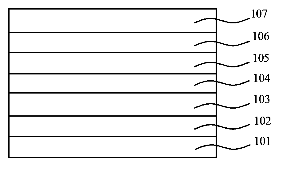
[0063] (2) Preparation of hole injection layer, hole transport layer, light emitting layer, electron transport layer, electron injection layer
[0064] Place the pretreated ITO substrate in a vacuum chamber (high vacuum coating system, Shenyang Scientific Instrument Development Center Co., Ltd.), and evacuate to 5×10 -3 Pa, with the vapor deposition rate of 1nm / s 2 o 5 Evaporated on the ITO substrate as a hole injection layer with a thickness of 50nm;
[0065] Evaporate TAPC on the hole injection layer as a hole transport layer at an evaporation rate of 1 nm / s, with a thickness of 40 nm;
[0066] Evaporate BCzVBi on the hole transport layer as a light...
Embodiment 2
[0074] A method for preparing an organic electroluminescent device, comprising the following steps:
[0075] (1) Conductive anode substrate pretreatment
[0076] The AZO substrate with a thickness of 80nm was ultrasonicated for 15 minutes with detergent and deionized water in order to remove organic pollutants on the glass surface.
[0077] (2) Preparation of hole injection layer, hole transport layer, light-emitting layer, electron transport layer, and electron injection layer. Place the pretreated AZO substrate in a vacuum chamber (high vacuum coating system, Shenyang Scientific Instrument Development Center Co., Ltd.) , evacuated to 2×10 -4 Pa, WO was deposited at a deposition rate of 10nm / s 3 Evaporated on the AZO substrate as a hole injection layer with a thickness of 80nm;
[0078] N,N'-diphenyl-N,N'-bis(1-naphthyl)-1,1'-biphenyl-4,4'-diamine (NPB) was deposited at a deposition rate of 0.1nm / s Evaporated on the hole injection layer as a hole transport layer with a th...
Embodiment 3
[0086] A method for preparing an organic electroluminescent device, comprising the following steps:
[0087] (1) Conductive anode substrate pretreatment
[0088] The IZO substrate with a thickness of 300nm was ultrasonicated for 15 minutes with detergent and deionized water in sequence to remove organic pollutants on the glass surface.
[0089] (2) Preparation of hole injection layer, hole transport layer, light emitting layer, electron transport layer, electron injection layer
[0090] Place the pretreated IZO substrate in a vacuum chamber (high vacuum coating system, Shenyang Scientific Instrument Development Center Co., Ltd.), and evacuate to 2.5×10 -3 Pa, MoO was deposited at a deposition rate of 5nm / s 3 Evaporated on the IZO substrate as a hole injection layer with a thickness of 40nm;
[0091] Evaporate TCTA on the hole injection layer as a hole transport layer at an evaporation rate of 0.5nm / s, and its thickness is 45nm;
[0092] Alq was deposited at a deposition ra...
PUM
| Property | Measurement | Unit |
|---|---|---|
| Particle size | aaaaa | aaaaa |
| Thickness | aaaaa | aaaaa |
| Thickness | aaaaa | aaaaa |
Abstract
Description
Claims
Application Information
 - R&D
- Intellectual Property
- Life Sciences
- Materials
- Tech Scout
- Unparalleled Data Quality
- Higher Quality Content
- 60% Fewer Hallucinations
Browse by: Latest US Patents, China's latest patents, Technical Efficacy Thesaurus, Application Domain, Technology Topic, Popular Technical Reports.
© 2025 PatSnap. All rights reserved.Legal|Privacy policy|Modern Slavery Act Transparency Statement|Sitemap|About US| Contact US: help@patsnap.com