Zinc-oxide-base amorphous oxide semiconductor thin film transistor and manufacturing method thereof

A technology of amorphous oxide and thin film transistors, which is applied in semiconductor/solid-state device manufacturing, transistors, semiconductor devices, etc., and can solve the problem of light transmittance of double-layer active layer structure, display circuit failure, and device electrical stability No high problems, to achieve the effect of improving mobility and working current, high local homogeneity of the film, and good stress balance

Inactive Publication Date: 2014-06-04
HUAZHONG UNIV OF SCI & TECH
View PDF3 Cites 4 Cited by
  • Summary
  • Abstract
  • Description
  • Claims
  • Application Information

AI Technical Summary

Problems solved by technology

[0004] Nevertheless, the double-layer active layer structure has the following problems: (1) The mismatch of crystal lattice and bandwidth leads to a large number of defect states near the interface of the double-layer active layer. Factors such as the defect state of the gate insulating layer and the charge trap at the interface between the insulating layer and the active layer, and photogenerated carriers will cause the threshold voltage of the device to drift, so that the display circuit cannot work normally, and the electrical stability of the device is not high.
(2) In terms of flexible display applications, if a double-layer active layer structure is used, when the device is bent and twisted, due to the lattice mismatch of the two-layer structure, the interface will generate a large stress, resulting in a large number of defects in some areas , and even cause the device to fail to work
(3) Due to the reflection of the interface, the light transmission of the double-layer active layer structure will be affected

Method used


Image

  • Zinc-oxide-base amorphous oxide semiconductor thin film transistor and manufacturing method thereof

Examples


Embodiment 1

[0034] A method for manufacturing a zinc oxide-based amorphous oxide semiconductor thin film transistor comprises the following steps:

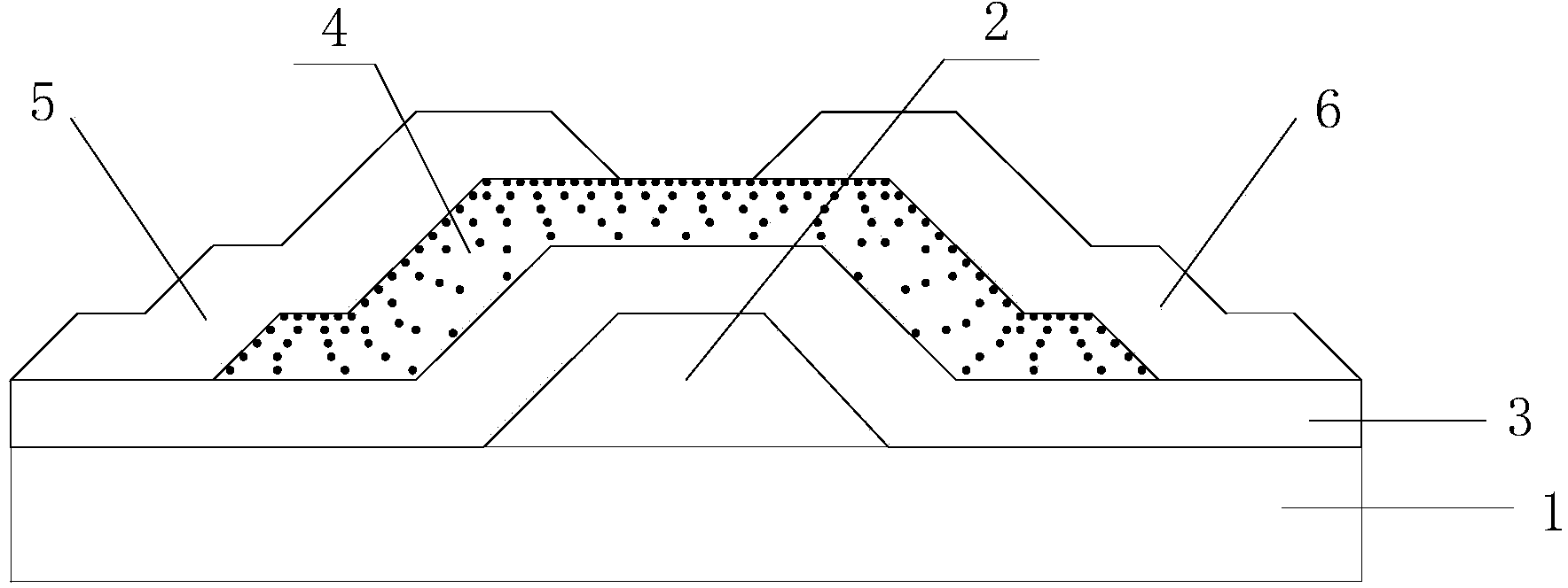
[0035](1) Deposit a layer of Mo with a thickness of 150 nm on a clean glass substrate by direct current sputtering, and etch to form a gate.

[0036] (2) PECVD grows a layer of SiO with a thickness of 50nm 2 A gate insulating layer covering the gate and the substrate.

[0037] (3) Simultaneously magnetron sputtering indium zinc oxide target (indium zinc molar ratio is 1:9) and gallium zinc oxide target ( The molar ratio of gallium to zinc is 9:1), the sputtering power applied to the indium zinc oxide target gradually decreases from 30W at the beginning to 0W at the end, and the sputtering power applied to the gallium zinc oxide target is determined by The 0W at the beginning gradually increased to 30W at the completion, the substrate rotation speed was 5rpm, and a 20nm-thick zinc oxide-based amorphous oxide semiconductor active layer doped ...

Embodiment 2

[0040] A method for manufacturing a zinc oxide-based amorphous oxide semiconductor thin film transistor comprises the following steps:

[0041] (1) Deposit a layer of Mo with a thickness of 150 nm on a clean glass substrate by direct current sputtering, and etch to form a gate.

[0042] (2) PECVD grows a layer of SiO with a thickness of 50nm 2 A gate insulating layer covering the gate and the substrate.

[0043] (3) Simultaneously magnetron sputtering indium zinc oxide target (indium zinc molar ratio is 9:1) and gallium zinc oxide target ( The ratio of gallium to zinc is 1:9), the sputtering power applied to the indium zinc oxide target gradually decreases from 400W at the beginning to 0W at the end, and the sputtering power applied to the gallium zinc oxide target starts from 0W at the time of completion gradually increased to 400W at the time of completion, the substrate rotation speed was 20rpm, and a layer of zinc oxide-based amorphous oxide semiconductor active layer do...

Embodiment 3

[0046] (1) Deposit a layer of Mo with a thickness of 150 nm on a clean glass substrate by direct current sputtering, and etch to form a gate.

[0047] (2) PECVD grows a SiO2 gate insulating layer with a thickness of 50nm, covering the gate and the substrate.

[0048] (3) Simultaneously magnetron sputtering indium zinc oxide target (indium zinc molar ratio is 4:3) and gallium zinc oxide target ( The ratio of gallium to zinc is 3:2), the sputtering power applied to the indium zinc oxide target gradually decreases from 300W at the beginning to 0W at the end, and the sputtering power applied to the gallium zinc oxide target starts from The 0W at the time of completion gradually increased to 300W at the time of completion, the substrate rotation speed was 10rpm, and a layer of zinc oxide-based amorphous oxide semiconductor active layer doped with indium and gallium was deposited with a thickness of 50nm.

[0049] (4) Deposit a layer of indium tin oxide with a thickness of 40 nm on...


PUM

PropertyMeasurementUnit
thicknessaaaaaaaaaa

Abstract

The invention discloses a zinc-oxide-base amorphous oxide semiconductor thin film transistor and a manufacturing method of the zinc-oxide-base amorphous oxide semiconductor thin film transistor. The zinc-oxide-base amorphous oxide semiconductor thin film transistor comprises a substrate, a grid electrode, a grid insulating layer, an active layer, a source electrode and a drain electrode, wherein the grid electrode is formed on the substrate, the grid electrode and the substrate are covered with the grid insulating layer, the active layer is formed on the grid insulating layer and corresponds to the grid electrode, and the two ends of the active layer are covered with the source electrode and the drain electrode respectively; a zinc-oxide-base amorphous oxide semiconductor doped with X and Y serves as the active layer, when the distance between the active layer and the grid insulating layer gradually increases, the content of the X gradually decreases, and the content of the Y gradually increases; the X is one of Cd, In, Sn, Sb, Ti, Pb and As, and the Y is one of Ga, Al, Hf, Ge, Ca and Cu. According to the zinc-oxide-base amorphous oxide semiconductor thin film transistor and the manufacturing method of the zinc-oxide-base amorphous oxide semiconductor thin film transistor, the mobility ratio of a device can be effectively improved, the magnitude of the working current of the device can be effectively improved, the frequency of the phenomenon of threshold voltage drift of the device is reduced, influence of the technology, illumination and gas in the outside world on the device is reduced, and mechanical stability of the device is improved.

Description

technical field [0001] The invention belongs to the technical field of flat panel display driving, and more specifically relates to a zinc oxide-based amorphous oxide semiconductor thin film transistor and a manufacturing method thereof. Background technique [0002] With the development of flat panel display technology, traditional silicon-based thin film transistors cannot meet the driving requirements of displays. For this reason, a thin film transistor using an amorphous metal oxide as an active layer has been proposed, which has the advantages of transparency, high mobility, and good uniformity. [0003] Since it is difficult for an amorphous metal oxide thin film transistor with a single active layer structure to balance high mobility and high electrical stability, in order to improve its electrical performance, some researchers have proposed a double-layer active layer structure. For example, using an indium tin oxide / indium gallium zinc oxide (ITO / IGZO) double-layer...

Claims


Application Information

Patent Timeline
Patent Type & Authority Applications(China)
IPC IPC(8): H01L29/786H01L29/227H01L29/22H01L21/34
CPCH01L29/7869H01L29/22H01L29/227H01L29/66742
Inventor 尹盛李小月徐东
Owner HUAZHONG UNIV OF SCI & TECH
Why Eureka
Try Eureka