Method for reducing e-SiGe lattice imperfections in PMOS manufacturing process

A technology of lattice defect and manufacturing process, which is applied in semiconductor/solid-state device manufacturing, electrical components, circuits, etc., can solve problems such as lattice defect and rework, so as to improve yield rate, reduce rework, shorten production cycle and production cost Effect

Active Publication Date: 2014-06-18
SHANGHAI HUALI MICROELECTRONICS CORP
View PDF5 Cites 4 Cited by
  • Summary
  • Abstract
  • Description
  • Claims
  • Application Information

AI Technical Summary

Problems solved by technology

[0012] Therefore, how to provide a method for reducing e-SiGe lattice defects in the PMOS manufacturing process, avoiding the lattice defects caused by the epitaxy and subsequent processes caused by the formation of a natural oxide layer before the silicon wafer is put into the epitaxy machine, and solving the existing problems at the same time Problems with processes that need to be reworked

Method used


Image

  • Method for reducing e-SiGe lattice imperfections in PMOS manufacturing process

Examples


no. 1 example

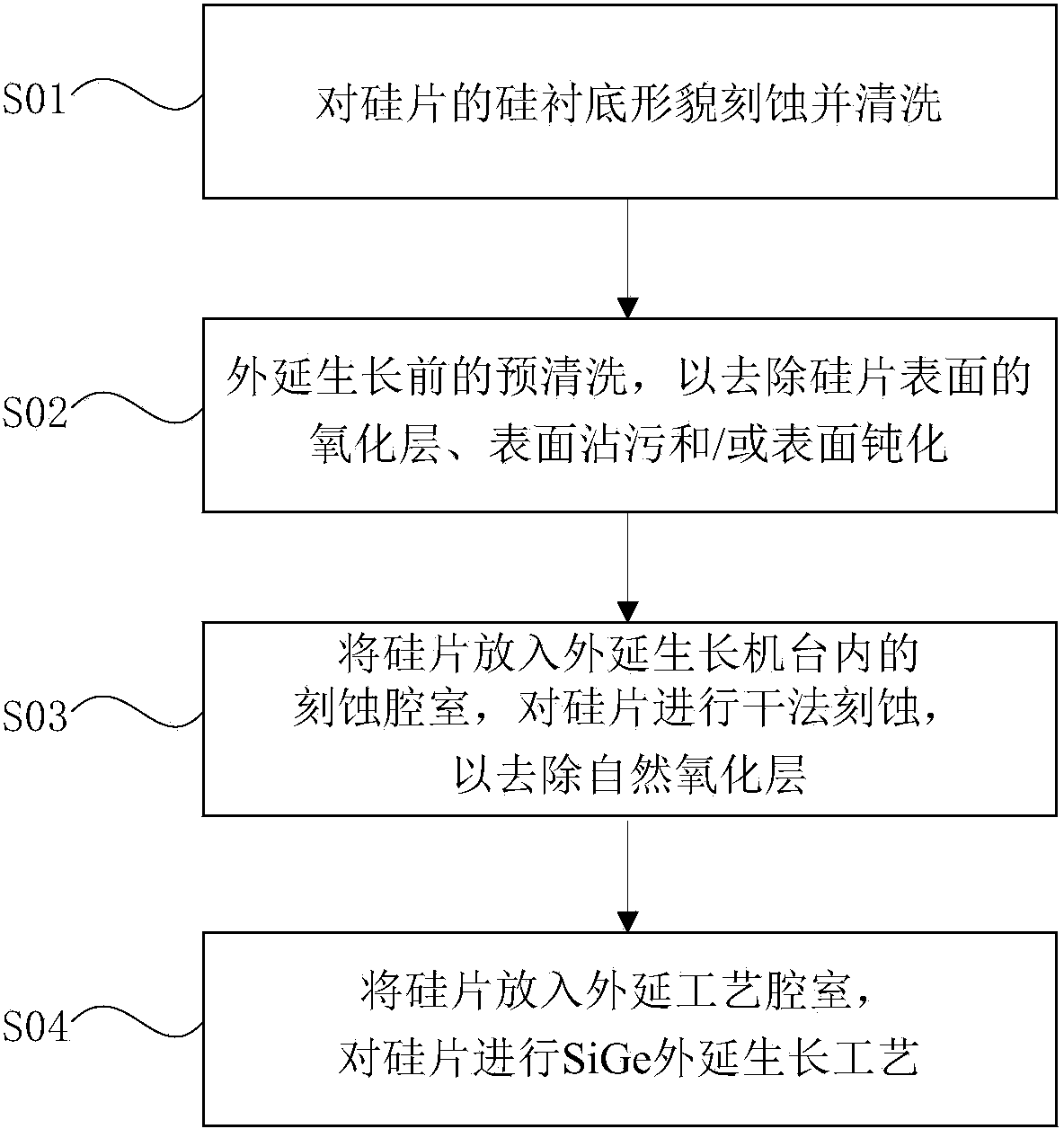
[0031] see figure 1 , the method for reducing e-SiGe lattice defects in the PMOS manufacturing process of this embodiment includes the following steps:

[0032] Step S01, etching and cleaning the topography of the silicon substrate of the silicon wafer. Among them, this step is completed on the etching machine, etching the silicon substrate to provide subsequent epitaxial growth of SiGe, cleaning is to remove the material remaining on the surface of the silicon wafer after etching, the cleaning medium can be deionized water, etc., this step It can be done by conventional means.

[0033] Step S02 , pre-cleaning before epitaxial growth, to remove the oxide layer, surface contamination and / or surface passivation on the surface of the silicon wafer. Among them, this step is completed on the cleaning machine, and the cleaning medium can be selected from DI-O 3 (Ozone-containing deionized water), SC-1 (Standard No. 1 solution, a mixed solution of ammonia, hydrogen peroxide and de...


PUM


Abstract

The invention discloses a method for reducing e-SiGe lattice imperfections in the PMOS manufacturing process. The method includes the steps of etching and cleaning the shape and the appearance of a silicon base of a silicon wafer, conducting pre-cleaning before extension growth, placing the silicon wafer into an etching chamber of an extension growth machine table, conducting dry etching on the silicon wafer so as to remove a natural oxidation layer, placing the silicon wafer into an extension process chamber, and conducting the SiGe extension growth process on the silicon wafer. Through in-situ etching on the natural oxidation layer, generated before the silicon wafer enters the extension growth machine table, of the silicon wafer, the lattice imperfections which are caused to the extension process and the subsequent process by the natural oxidation layer are avoided, and therefore device failures are reduced, and the yield of the silicon wafer is improved; meanwhile, rework in the process production is reduced, the production cycle of the product is shortened, and production cost of the product is reduced.

Description

technical field [0001] The invention relates to the technical field of semiconductor integrated circuit manufacturing technology, in particular to a method for reducing e-SiGe (embedded silicon germanium) lattice defects in a PMOS manufacturing technology. Background technique [0002] Today, semiconductor integrated circuit technology is advancing very rapidly. According to Moore's Law, the feature size of integrated circuits will decrease by 30% every 18 months, while the integration level will double. In the advanced CMOS (Complementary Metal Oxide Semiconductor, Complementary Metal Oxide Semiconductor) integrated circuit process, the traditional method of reducing the thickness of the gate oxide layer can no longer meet the needs of the device. Therefore, people have to use other methods to improve device performance, such as high dielectric constant gate oxide technology and stress enhancement technology. [0003] The most important thing in the stress enhancement meth...

Claims


Application Information

Patent Timeline
IPC IPC(8): H01L21/20H01L21/336
CPCH01L21/02043H01L21/02046
Inventor 曹威江润峰
Owner SHANGHAI HUALI MICROELECTRONICS CORP
Why Eureka
Try Eureka