

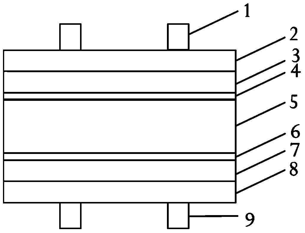
HIT solar cell and preparing method thereof
A technology of solar cells and batteries, which is applied in the field of solar cells, can solve problems such as high cost and reduce production costs, and achieve the effects of reducing production costs and improving plane utilization
- Summary
- Abstract
- Description
- Claims
- Application Information
AI Technical Summary
Problems solved by technology
Method used
Image

Examples
Embodiment 1
[0030] The preparation process of the HIT solar cell structure mainly includes:
[0031] 1) Cleaning process
[0032] Use the standard RCA cleaning process to treat the P-type polysilicon substrate to remove particles, organic matter and metal impurities on the surface of the P-type polysilicon substrate. The polysilicon substrate used in this experiment has a thickness of 117um, a resistivity of 2.5Ω cm, and a minority The lifespan is 1.1us. After cleaning, the minority carrier diffusion length of the polysilicon wafer measured by ELYMAT technology is 31.18 μm;
[0033] 2) Aluminum gettering process
[0034] First, use a vacuum coating machine to vapor-deposit an aluminum layer with a thickness of 1.3 μm on any side of the P-type polysilicon substrate by thermal evaporation (the evaporated aluminum side is the front side of the silicon wafer). Then anneal the silicon wafer: raise it from room temperature to 800°C in an argon atmosphere, then keep it warm for two hours, the...
Embodiment 2
[0044] The other steps of this embodiment are the same as those of Embodiment 1, the difference is the aluminum gettering process in step 2):
[0045] First, an aluminum layer with a thickness of 1-2 μm is vapor-deposited on any surface of the cleaned P-type polysilicon substrate, and the evaporated aluminum surface is the front of the silicon wafer; The temperature was raised to 700°C, kept for 3 hours, then annealed and cooled to room temperature, the heating rate and cooling rate were both 5°C / min; then the P-type polysilicon substrate was soaked in NaOH solution with a mass fraction of 10% for 20 minutes, The aluminum layer and alloy layer on the surface are etched away.
[0046] The obtained HIT solar cell utilizes an instrument (KEITHLEY-2611) at a power of 100mV / cm 2 Under white light irradiation, the measured efficiency is 18.5%.
Embodiment 3
[0048] The other steps of this embodiment are the same as those of Embodiment 1, the difference is the aluminum gettering process in step 2):
[0049] First, an aluminum layer with a thickness of 1-2 μm is evaporated on any surface of the cleaned P-type polysilicon substrate, and the evaporated aluminum surface is the front side of the silicon wafer; Raise to 750°C, hold for 3 hours, then anneal and cool down to room temperature, the heating rate and cooling rate are both 10°C / min; then soak the P-type polysilicon substrate with 10% NaOH solution for 20 minutes, etch Remove the aluminum layer and alloy layer on the surface. The performance of the battery is the same as in Example 2.
[0050] As can be seen from Table 1, the present invention uses a polycrystalline silicon wafer as a substrate, and while the cell efficiency basically reaches the domestic advanced level, the cost is greatly reduced (the price of a two-inch double-throwing monocrystalline silicon wafer with a th...
PUM
| Property | Measurement | Unit |
|---|---|---|
| thickness | aaaaa | aaaaa |
| thickness | aaaaa | aaaaa |
| thickness | aaaaa | aaaaa |
Abstract
Description
Claims
Application Information