Micro nano structure solar battery and preparation method of back light trapping structure thereof

A technology of a solar cell and a light trapping structure, applied in the field of solar cells, can solve the problems of uneven deposition in a deposition process, and achieve the effects of improving short-circuit current and conversion efficiency, increasing optical path, and realizing light scattering.

Active Publication Date: 2014-07-23
SHANGHAI JIAO TONG UNIV
View PDF11 Cites 12 Cited by
  • Summary
  • Abstract
  • Description
  • Claims
  • Application Information

AI Technical Summary

Problems solved by technology

[0006] In view of the shortcomings of the prior art described above, the purpose of the present invention is to provide a method for preparing a micro-nano structured solar cell and its back light-trapping structure, which is used to solve the problems caused by the existence of edges and corners of the back light-trapping structure of the solar cell in the prior art. Subsequent deposition process has problems such as uneven deposition

Method used


Image

  • Micro nano structure solar battery and preparation method of back light trapping structure thereof
  • Micro nano structure solar battery and preparation method of back light trapping structure thereof
  • Micro nano structure solar battery and preparation method of back light trapping structure thereof

Examples


Embodiment 1

[0038] The invention provides a method for preparing a light-trapping structure on the back of a micro-nano structured solar cell, which specifically includes the following steps:

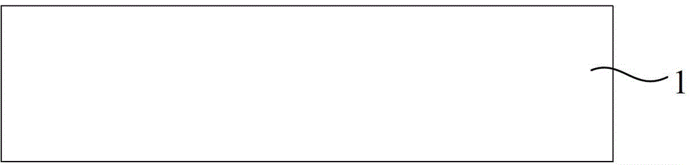
[0039] (1) A glass substrate 1 is provided.

[0040] see figure 1 . Before performing subsequent processes, the provided glass substrate 1 can be cleaned to remove impurities on the glass substrate 1 and avoid affecting the photoelectric conversion performance of the solar cell.

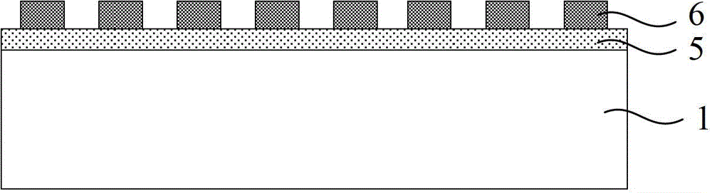
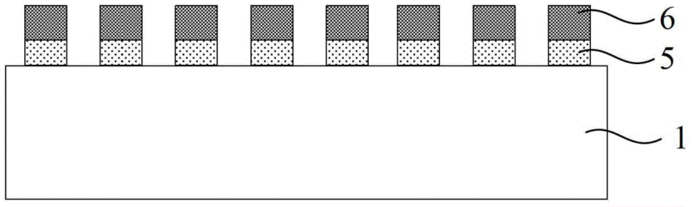
[0041] (2) Etching the glass substrate 1 by using an etching process, so that the surface of the glass substrate 1 is a columnar array structure 11;

[0042]This step includes the following steps: first prepare and form a metal layer 5 on the glass substrate 1; then apply a photoresist layer 6 on the metal layer 5, and obtain the required photoresist pattern by photolithography; The metal layer 5 and the glass substrate 1 are etched by an etching process; after the metal layer is removed, the glass substrate 1 with a c...

Embodiment 2

[0057] The difference between this embodiment and Embodiment 1 is that the process parameters for preparing the light-trapping structure are different, as follows:

[0058] 1) A glass substrate is used as a substrate, and a metal layer is deposited on the glass substrate as a mask layer. The metal layer is metal such as Cr with a thickness of 70nm.

[0059] 2) The desired photoresist pattern is obtained on the glass substrate by using photolithography technology of contact ultraviolet exposure, and the line width of the photoresist pattern is 700 nm.

[0060] 3) Use the photoresist as a mask to wet-etch the window of the metal layer. The composition ratio of the mixed solution used is: in every 100ml of etching solution, cerium ammonium nitrate is 11g, perchloric acid is 4.4ml, The balance is water.

[0061] 4) Using reactive ion etching technology to etch the glass substrate, the reaction gas is CHF 3 , the flow rate is 30 sccm, and the aspect ratio of the pattern etched i...

Embodiment 3

[0066] The difference between this embodiment and Embodiments 1 and 2 is that the process parameters for preparing the light-trapping structure are different, as follows:

[0067] 1) A glass substrate is used as a substrate, and a metal layer is deposited on the glass substrate as a mask layer. The metal layer is metal such as Cr with a thickness of 80nm.

[0068] 2) The required photoresist pattern is obtained on the glass substrate by using the photolithography technology of contact ultraviolet exposure, and the line width of the photoresist pattern is 800nm.

[0069] 3) Use the photoresist as a mask to wet-etch the window of the metal layer. The composition ratio of the mixed solution used is: in every 100ml of etching solution, cerium ammonium nitrate is 14g, perchloric acid is 5.6ml, The balance is water.

[0070] 4) Using reactive ion etching technology to etch the glass substrate, the reaction gas is CHF 3 , the flow rate is 30 sccm, and the aspect ratio of the patte...


PUM

PropertyMeasurementUnit
thicknessaaaaaaaaaa
thicknessaaaaaaaaaa
widthaaaaaaaaaa

Abstract

The invention provides a micro nano structure solar battery and the preparation method of a back light trapping structure thereof. The method comprises the steps that a glass substrate is provided; an etching process is used to etch the glass substrate, so that the surface of the glass substrate is in a columnar array structure; and an ion beam etching technology is used and a predetermined angle is rotated, so that the glass substrate whose surface is in an angle-free periodic micro nano structure is acquired, and the angle-free periodic micro nano structure is the light trapping structure. According to the invention, the light trapping structure is located on the back of the solar battery; through reflection, refraction and scattering of the structure, the optical distance of a light in the solar battery is increased; and after the reactive ion etching technology and the ion beam etching technology are used to acquire the angle-free periodic micro nano light trapping structure on the surface, the problems of nonuniform deposition, conductive layer disconnection and the like are avoided when subsequent electrode and silica-based film deposition is carried out.

Description

technical field [0001] The invention relates to the technical field of solar cells, in particular to a preparation method of a micro-nano structured solar cell and a back light-trapping structure thereof. Background technique [0002] The light loss in amorphous silicon thin film solar cells mainly comes from the following three aspects: the loss of surface reflection; the loss of the total energy of incident light due to the coverage area of ​​the electrode material on the light-incoming surface; and the transmission loss caused by the thin thickness of the cell. Introducing a light-trapping structure into the cell can effectively reduce the thickness of the absorbing layer, thereby reducing the deposition time. In the p-i-n structure amorphous silicon thin film solar cell, the light trapping structure is realized by combining the micro-nano structure of the front electrode and the high back reflection electrode. By using a substrate with a micro-nano structure, the incide...

Claims


Application Information

Patent Timeline
Patent Type & Authority Applications(China)
IPC IPC(8): H01L31/18H01L31/0236
CPCH01L31/02366Y02E10/50Y02P70/50
Inventor 李海华王庆康
Owner SHANGHAI JIAO TONG UNIV
Why Eureka
Try Eureka