

Manufacturing method of solar energy battery
A solar cell and manufacturing method technology, applied to circuits, photovoltaic power generation, electrical components, etc., can solve the problems of expensive equipment, high operating costs, and high process complexity, so as to reduce manufacturing costs, solve alignment problems, and simplify process steps. Effect
- Summary
- Abstract
- Description
- Claims
- Application Information
AI Technical Summary
Problems solved by technology
Method used
Image

Examples
Embodiment 1
[0044] refer to Figure 1-5 , the manufacture method of the solar cell described in the present embodiment is as follows:
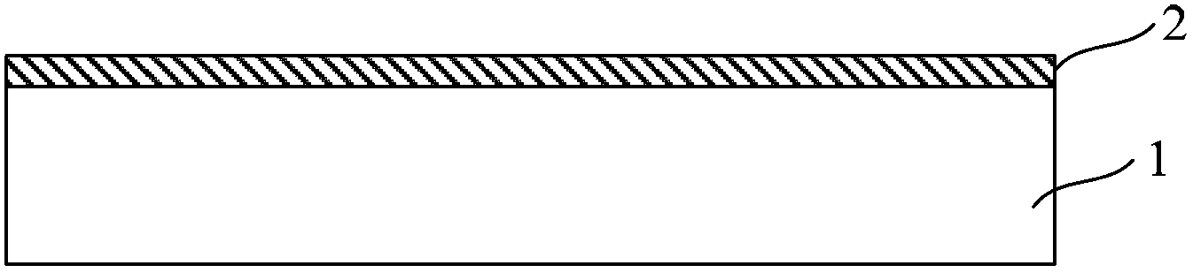
[0045] Such as figure 1 As shown, a substrate is provided, which is a commercially available silicon wafer used for making solar cells. After texturizing the front side of the silicon wafer 1 , a P-type heavily doped layer 2 is formed on the entire back side of the silicon wafer 1 . When the IBC battery is in use, the front side receives light, and the back side is provided with electrodes. However, due to the practice in the field, the upper side is the back side and the lower side is the front side. This is well known to those skilled in the art.
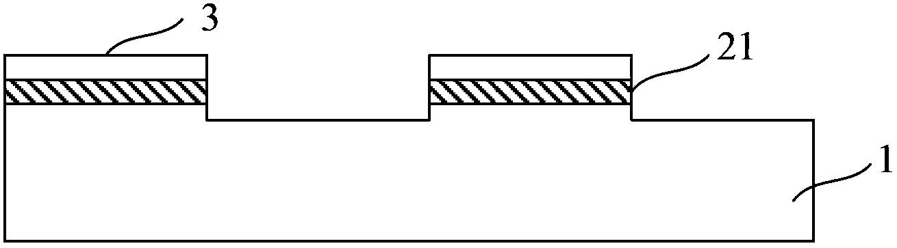
[0046] Such as figure 2As shown, a mask 3 is formed on the entire back surface of the silicon wafer 1, and the area not covered by the mask 3 is an open area. Specifically, the specific formation method of the mask 3 may be to first apply a mask layer on the back surface, then form a pattern protective la...
Embodiment 2
[0054] The principle of embodiment 2 is the same as that of embodiment 1, the difference is:
[0055] A physical method such as laser ablation is used to etch the part not covered by the mask to form the groove, and then a chemical method (such as wet chemical etching) is used to remove the damaged layer left by the physical method.
[0056] All the other unmentioned steps are the same as in Example 1.
Embodiment 3
[0058] The principle of embodiment 3 is the same as that of embodiment 1, the difference is:
[0059] In the manufacturing process of the solar battery, a step of forming an anti-reflection layer on the front surface of the silicon chip is also included.
[0060] All the other unmentioned steps are the same as in Example 1.
PUM
| Property | Measurement | Unit |
|---|---|---|
| Thickness | aaaaa | aaaaa |
| Depth | aaaaa | aaaaa |
| Thickness | aaaaa | aaaaa |
Abstract
Description
Claims
Application Information