Production method for semiconductor device, production device for semiconductor device, and storage medium

A manufacturing method and manufacturing device technology, applied in semiconductor/solid-state device manufacturing, semiconductor devices, electric solid-state devices, etc., to achieve the effect of improving film quality

Active Publication Date: 2014-08-20
KOKUSA ELECTRIC CO LTD
View PDF7 Cites 2 Cited by
  • Summary
  • Abstract
  • Description
  • Claims
  • Application Information

AI Technical Summary

Problems solved by technology

However, silicon materials such as polysilazane are known to contain nitrogen as an impurity due to ammonia

Method used


Image

  • Production method for semiconductor device, production device for semiconductor device, and storage medium
  • Production method for semiconductor device, production device for semiconductor device, and storage medium
  • Production method for semiconductor device, production device for semiconductor device, and storage medium

Examples


Embodiment

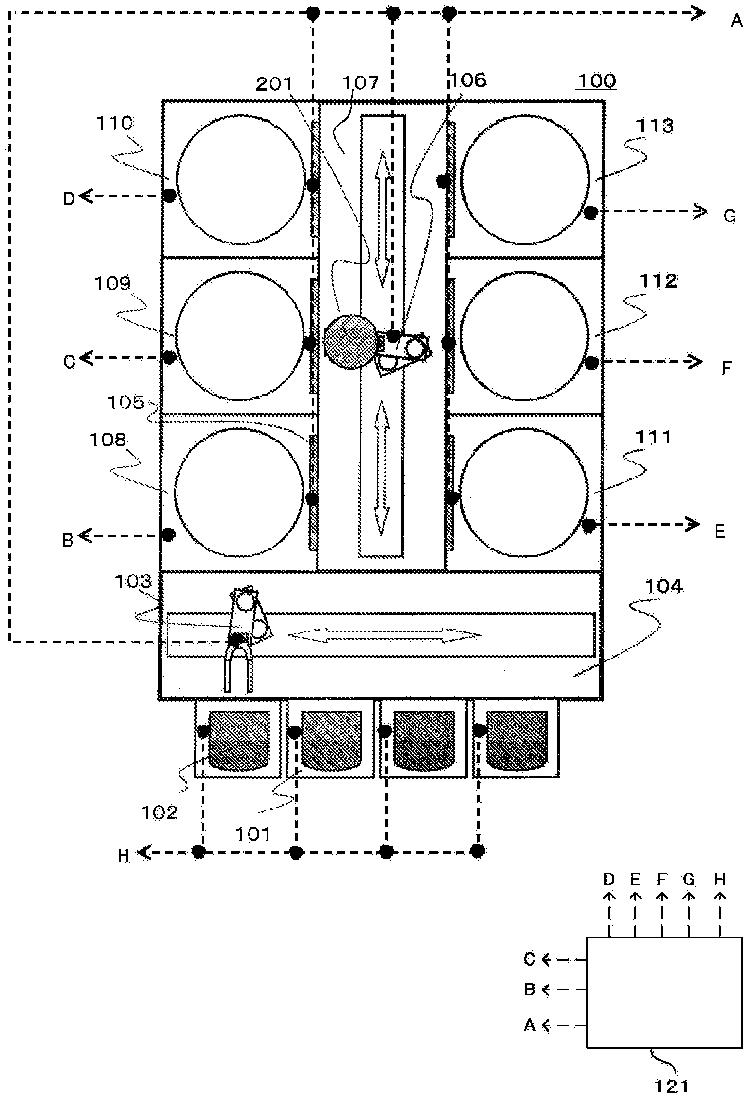
[0195] Next, while referring to Figure 14 ~ Figure 16 Embodiments of the present invention will be described.

[0196] In this embodiment, a wafer 201 having a silicon-containing film containing polysilazane is used. The film thickness of the silicon-containing film was 600 nm. First, a curing treatment (pre-baking treatment) is performed on a wafer 201 having a silicon-containing film (Example 1).

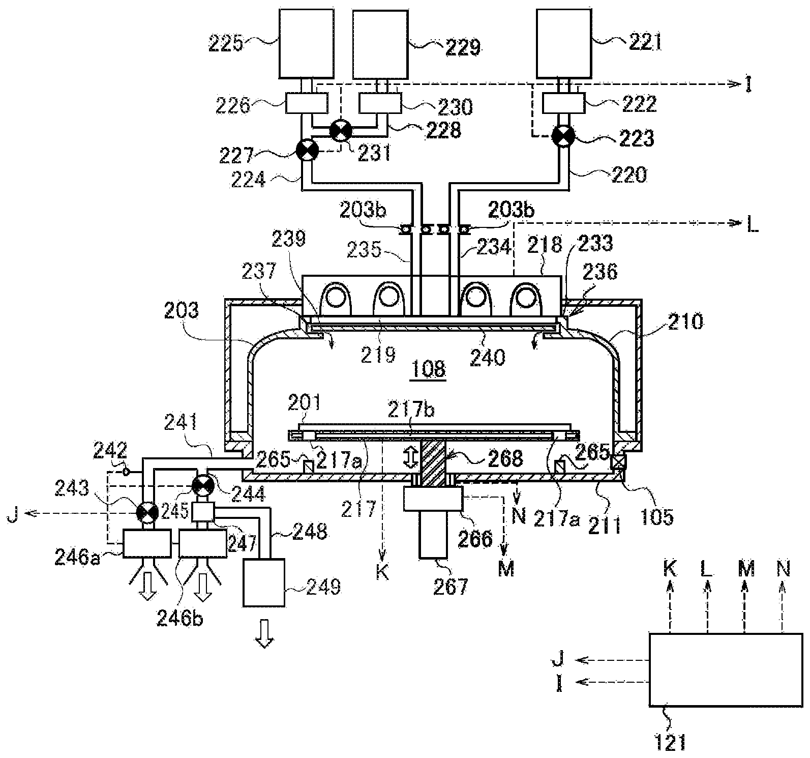
[0197] In addition, the cured wafer 201 (wafer 201 of Example 1) having a silicon-containing film was subjected to oxidation treatment (hydrogen peroxide treatment, atmospheric pressure peroxidation treatment) in the treatment chamber 108 at 50° C. and atmospheric pressure. hydrogen water treatment) (embodiment 2). In addition, in the oxidation treatment, hydrogen peroxide water having a hydrogen peroxide concentration of 30 wt % was used as an oxidizing agent solution, and was performed for 30 minutes.

[0198] In addition, pure water treatment was performed by supplying pur...


PUM


Abstract

Provided is a method of manufacturing a semiconductor device. The method includes (a) loading a substrate having a silicon-containing film formed thereon into a process chamber; (b) supplying a gas into the process chamber from a gas supply unit until an inner pressure of the process chamber is equal to or greater than atmospheric pressure; and (c) supplying a process liquid from a process liquid supply unit to the substrate to oxidize the silicon-containing film.

Description

technical field [0001] The present invention relates to a method for manufacturing a semiconductor device, a device for manufacturing a semiconductor device, and a recording medium. Background technique [0002] With the miniaturization of semiconductor devices such as large scale integrated circuits (hereinafter referred to as LSI), technical difficulties in processing technologies for controlling leakage current interference between transistor elements have gradually increased. Generally, LSI element-to-element isolation is performed by forming a space such as a groove or a hole between elements to be separated on a substrate such as a silicon substrate made of silicon (Si), and depositing insulating material in the space. things. As the insulator, an oxide film is often used. As the oxide film, for example, a silicon oxide film can be used. The silicon oxide film is formed on the substrate by natural oxidation of the silicon substrate itself or by chemical vapor deposi...

Claims


Application Information

Patent Timeline
Patent Type & Authority Applications(China)
IPC IPC(8): H01L21/316H01L21/336H01L21/8242H01L21/8247H01L27/108H01L27/115H01L29/788H01L29/792
CPCH01L21/02164H01L21/02222H01L21/67207H01L21/02255H01L21/02326H01L21/02282C23C16/56H01L21/67115H01L21/67017H01L21/02236H01L21/02343
Inventor 芦原洋司天野富大桧山真佐久间春信和田优一立野秀人
Owner KOKUSA ELECTRIC CO LTD
Why Eureka
Try Eureka